
Key facts
- Brand
- Analog Devices
- Model
- ADCLK846
- Category
- Other
- Industry
- Electronics
- Documents
- 3
- Languages
- EN
- Last added
- 2026-09-29
Start here
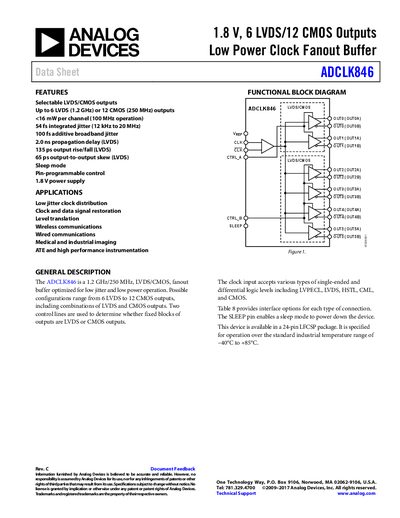
Analog Devices ADCLK846 Clock Fanout Buffer Data Sheet
The ADCLK846 provides selectable LVDS or CMOS outputs for clock distribution, supporting up to 6 LVDS (1.2 GHz) or 12 CMOS (250 MHz) channels. It operates from a 1.8 V supply and includes a sleep mode to reduce power consumption.
Designed for low jitter applications, the device delivers 54 fs integrated random jitter and 100 fs additive broadband jitter. It is supplied in a 24‑pin LFCSP package and is rated for an industrial temperature range of –40 °C to +85 °C.
Analog Devices ADCLK846 specifications
| Supply voltage (VS) | 1.71 V – 1.89 V |
|---|---|
| LVDS output frequency | Up to 1200 MHz |
| CMOS output frequency | Up to 250 MHz |
| LVDS propagation delay (CLK‑to‑LVDS) | 1.5 ns – 2.0 ns |
| LVDS rise/fall time | 135 ps – 235 ps |
| LVDS output skew (same part) | 65 ps |
| Integrated random jitter (LVDS) | 54 fs rms |
| Sleep mode current | 3 mA |
Source: Analog Devices ADCLK846 Clock Fanout Buffer Data Sheet
All Analog Devices ADCLK846 documents by type
Ratings, dimensions and ordering codes, for selection and design work.
Questions answered in these manuals
How many LVDS outputs does the ADCLK846 provide?
It can provide up to six LVDS outputs.
From: Analog Devices ADCLK846 Clock Fanout Buffer Data Sheet
What is the operating temperature range of the ADCLK846?
The device is specified for –40 °C to +85 °C.
From: Analog Devices ADCLK846 Clock Fanout Buffer Data Sheet
What does the SLEEP pin do?
The SLEEP pin enables a sleep mode that turns off the device to reduce power consumption.
From: Analog Devices ADCLK846 Low‑Power Clock Fan‑Out Buffer Datasheet
How many LVDS and CMOS outputs can the ADCLK846 provide?
It can provide up to six LVDS outputs or twelve CMOS outputs, with configurable combinations.
From: Analog Devices ADCLK846 Low‑Power Clock Fan‑Out Buffer Datasheet
What supply voltage does the ADCLK846 require?
The device operates from 1.71 V to 1.89 V, with a typical value of 1.8 V.
What is the integrated random jitter for LVDS outputs?
The integrated random jitter is 54 fs rms (12 kHz to 20 MHz bandwidth).