
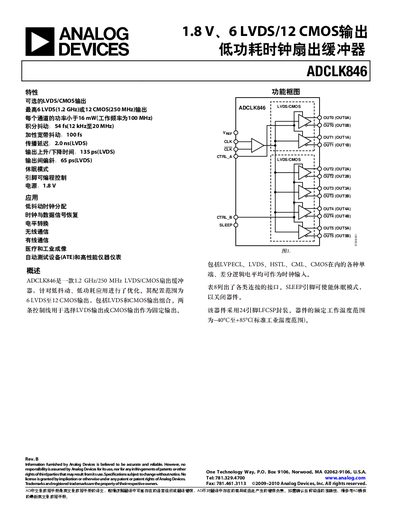
The ADCLK846 is a low‑jitter, low‑power clock fan‑out buffer optimized for high‑speed applications. It supports configurable LVDS and CMOS output combinations, with up to six LVDS or twelve CMOS channels and programmable control pins for output mode and sleep operation.
The device is supplied in a 24‑pin LFCSP package, operates from a 1.8 V supply, and is rated for an industrial temperature range of –40 °C to +85 °C. Detailed electrical, timing, and clock specifications are provided, along with pin descriptions and application guidance for clock distribution, level conversion, and high‑performance instrumentation.
| Maximum LVDS output frequency | 1.2 GHz |
|---|---|
| Maximum CMOS output frequency | 250 MHz |
| Power consumption per channel (100 MHz) | <16 mW |
| Operating temperature range | -40 °C to +85 °C |
| Junction‑to‑ambient thermal resistance (θJA) | 57.0 °C/W |
The SLEEP pin enables a sleep mode that turns off the device to reduce power consumption.
It can provide up to six LVDS outputs or twelve CMOS outputs, with configurable combinations.