
ADCLK846 is a low power clock fanout buffer with selectable LVDS/CMOS outputs. It can provide up to 6 LVDS (1.2 GHz) or 12 CMOS (250 MHz) outputs. Each channel consumes less than 16 mW power and has an integrated jitter of 54 fs (12 kHz to 20 MHz) and additive broadband jitter of 100 fs. It has a propagation delay of 2.0 ns (LVDS), output rise/fall time of 135 ps (LVDS), and output-to-output skew of 65 ps (LVDS). This product is suitable for applications such as low jitter clock distribution, clock and data signal restoration, level translation, wireless communications, wired communications, medical and industrial imaging, ATE, and high performance instrumentation.
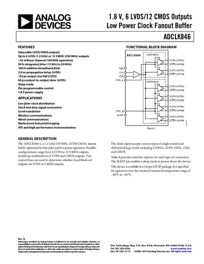
The ADCLK846 provides selectable LVDS or CMOS outputs, supporting up to six LVDS channels at 1.2 GHz or twelve CMOS channels at 250 MHz. It operates from a 1.8 V supply and consumes less than 16 mW per channel at 100 MHz, offering integrated jitter as low as 54 fs rms.
The device is supplied in a 24‑lead LFCSP package, rated for an industrial temperature range of –40 °C to +85 °C. Control pins allow configuration of output type and a sleep mode for power saving. Detailed electrical, timing, and thermal specifications are provided for design integration.
| CMOS Output Frequency | 250 MHz |
|---|---|
| Supply Voltage | 1.71 V – 1.89 V (typ. 1.8 V) |
| Power Consumption per Channel | <16 mW (100 MHz operation) |
| Integrated Random Jitter (LVDS) | 54 fs rms |
| Output Rise/Fall Time (LVDS) | 135 ps typ |
| Output Skew (LVDS, same part) | 65 ps |
| Operating Temperature Range | –40 °C to +85 °C |
The device operates from 1.71 V to 1.89 V, with a typical value of 1.8 V.
The integrated random jitter is 54 fs rms (12 kHz to 20 MHz bandwidth).
The device is rated for –40 °C to +85 °C ambient temperature.