
The ADCLK846 is a low‑power clock fanout buffer offering up to 6 LVDS or 12 CMOS outputs with sub‑100 fs jitter.
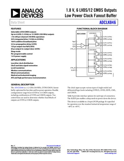
The ADCLK846 provides selectable LVDS or CMOS outputs for clock distribution, supporting up to 6 LVDS (1.2 GHz) or 12 CMOS (250 MHz) channels. It operates from a 1.8 V supply and includes a sleep mode to reduce power consumption.
Designed for low jitter applications, the device delivers 54 fs integrated random jitter and 100 fs additive broadband jitter. It is supplied in a 24‑pin LFCSP package and is rated for an industrial temperature range of –40 °C to +85 °C.
| Supply voltage (VS) | 1.71 V – 1.89 V |
|---|---|
| LVDS output frequency | Up to 1200 MHz |
| CMOS output frequency | Up to 250 MHz |
| LVDS propagation delay (CLK‑to‑LVDS) | 1.5 ns – 2.0 ns |
| LVDS rise/fall time | 135 ps – 235 ps |
| LVDS output skew (same part) | 65 ps |
| Integrated random jitter (LVDS) | 54 fs rms |
| Sleep mode current | 3 mA |
It can provide up to six LVDS outputs.
The device is specified for –40 °C to +85 °C.