
This user guide describes how to set up and use the ADCLK846 evaluation board. The ADCLK846 data sheet contains full technical details about the specifications and operation of this device and should be consulted when using the evaluation board. The ADCLK846 is a high performance clock fanout buffer. The evaluation board is fabricated using a high quality Rogers® dielectric material. Transmission line paths are kept as close to 100 Ω differentially as possible.
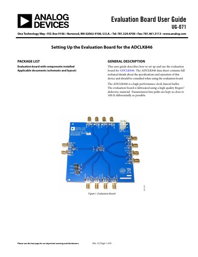
This user guide explains how to set up and use the ADCLK846 evaluation board. The board is fabricated using high-quality Rogers dielectric material to maintain transmission line paths as close to 100 Ω differential impedance as possible. It is intended for device evaluation and not for production purposes.
| Input Voltage Range | 0.15 V to 1.8 V |
|---|---|
| Supply Voltage | 1.8 V |
| Output Configuration | 6 differential LVDS or 12 single-ended 1.8 V CMOS |
The recommended setup sets the supply voltage (V S) to 1.8 V.
Required equipment includes a single power supply, signal source, high bandwidth oscilloscope, high bandwidth differential probe, and matched high speed cables.