
Key facts
- Brand
- Analog Devices
- Model
- AD9866
- Industry
- Industrial
- Documents
- 2
- Languages
- EN
- Last added
- 2012-05-09
Start here
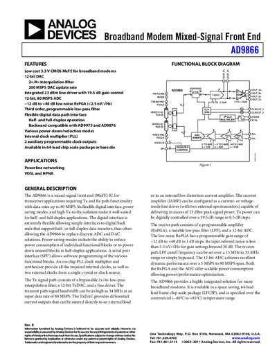
Analog Devices AD9866 Datasheet Rev B
The AD9866 integrates a 12‑bit DAC, 12‑bit ADC, programmable gain amplifiers, and a PLL‑based clock multiplier in a 64‑lead LFCSP package. It supports half‑ and full‑duplex operation, 3.3 V CMOS supply, and offers flexible digital interfaces for both half‑ and full‑duplex data paths.
The datasheet provides detailed specifications for the Tx and Rx paths, power‑supply requirements, digital timing, and pin configurations, along with ordering information and mechanical dimensions.
Analog Devices AD9866 specifications
| DAC Resolution | 12 bits |
|---|---|
| DAC Update Rate | 200 MSPS |
| ADC Resolution | 12 bits |
| ADC Conversion Rate | 80 MSPS |
| Supply Voltage (AVDD) | 3.3 V ±5 % |
| Total Supply Current (typ) | 475 mA |
| Operating Temperature Range | -40 °C to +85 °C |
| Package | 64‑lead LFCSP (LFCSP_VQ) |
All Analog Devices AD9866 documents by type
Ratings, dimensions and ordering codes, for selection and design work.
Questions answered in these manuals
What is the maximum DAC update rate of the AD9866?
The DAC can update at up to 200 MSPS.
What temperature range does the AD9866 support?
It operates from –40 °C to +85 °C.
What is the DAC update rate of the AD9866?
The DAC operates at a full‑scale update rate of 200 MSPS.
From: Analog Devices AD9866 Mixed‑Signal Front‑End Datasheet
What supply voltage does the AD9866 require?
The analog supply (AVDD) is 3.3 V with a tolerance of ±5 %.
From: Analog Devices AD9866 Mixed‑Signal Front‑End Datasheet