
Key facts
- Brand
- Fairchild
- Model
- FQT4N25
- Industry
- Industrial
- Documents
- 3
- Languages
- EN
- Last added
- 2012-07-12
Start here
Fairchild FQT4N25 N-Channel MOSFET Datasheet
Datasheet 8 pages · 654 KB · EN
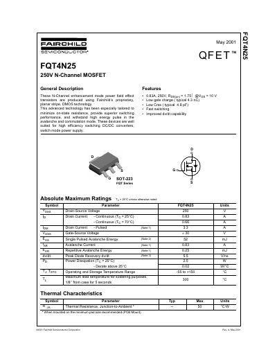
This document is a technical datasheet for the Fairchild Semiconductor FQT4N25, an N-Channel enhancement mode power field effect transistor. The device utilizes proprietary planar stripe DMOS technology designed to minimize on-state resistance while providing superior switching performance and high energy pulse tolerance in avalanche and commutation modes.
Read onlineFairchild FQT4N25 specifications
| Drain-Source Voltage (VDSS) | 250 V |
|---|---|
| Continuous Drain Current (ID) @ TC = 25°C | 0.83 A |
| Static Drain-Source On-Resistance (RDS(on)) @ VGS=10V | 1.75 Ω |
| Total Gate Charge (Qg) | 4.3 nC |
| Reverse Transfer Capacitance (Crss) | 4.8 pF |
| Operating Temperature Range | -55 to +150 °C |
All Fairchild FQT4N25 documents by type
Datasheet 1
Ratings, dimensions and ordering codes, for selection and design work.
Questions answered in these manuals
What is the maximum drain-source voltage of the FQT4N25?
The maximum drain-source voltage (VDSS) for the FQT4N25 is 250 V.
What package type does this MOSFET use?
The device uses a SOT-223 package.
What is the maximum drain‑source voltage of the FQT4N25?
The device is rated for a maximum drain‑source voltage of 250 V.
What continuous drain current can the FQT4N25 handle at 25 °C?
It can conduct up to 0.83 A continuously at a junction temperature of 25 °C.
What is the maximum drain‑source voltage of the FQT4N25?
The maximum drain‑source voltage is 250 V.
What is the typical gate charge for this MOSFET?
The typical gate charge is 4.3 nC.