
Key facts
- Brand
- Fairchild
- Model
- FDD6N50
- Category
- Other Electronics
- Documents
- 2
- Languages
- EN
- Last added
- 2012-07-11
Start here
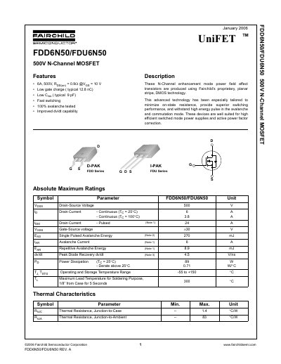
Fairchild Semiconductor FDD6N50/FDU6N50 500V N-Channel MOSFET Datasheet
The document describes the Fairchild FDD6N50/FDU6N50, a 500V N-Channel enhancement mode power field effect transistor produced using the company's proprietary UniFET technology. These devices are designed for high-efficiency switched mode power supplies and active power factor correction applications.
Read onlineFairchild FDD6N50 specifications
| Drain-Source Voltage | 500 V |
|---|---|
| On-Resistance | 0.9 Ω @VGS = 10 V |
| Gate Charge (Typical) | 12.8 nC |
| Reverse Transfer Capacitance (Typical) | 9 pF |
| Operating Temperature Range | -55 to +150 °C |
| Thermal Resistance Junction-to-Case | 1.4 °C/W |
Source: Fairchild Semiconductor FDD6N50/FDU6N50 500V N-Channel MOSFET Datasheet
All Fairchild FDD6N50 documents by type
Ratings, dimensions and ordering codes, for selection and design work.
Questions answered in these manuals
What is the maximum drain-source voltage?
The maximum drain-source voltage is 500 V.
From: Fairchild Semiconductor FDD6N50/FDU6N50 500V N-Channel MOSFET Datasheet
What is the typical on-resistance?
The typical on-resistance is 0.9 Ω at VGS = 10 V.
From: Fairchild Semiconductor FDD6N50/FDU6N50 500V N-Channel MOSFET Datasheet
What is the operating and storage temperature range?
The operating and storage temperature range is from -55 to +150 °C.
From: Fairchild Semiconductor FDD6N50F/FDU6N50F N-Channel MOSFET Datasheet