
Key facts
- Brand
- Fairchild
- Model
- FDS6892A
- Category
- Other Electronics
- Documents
- 2
- Languages
- EN
- Last added
- 2012-07-12
Start here
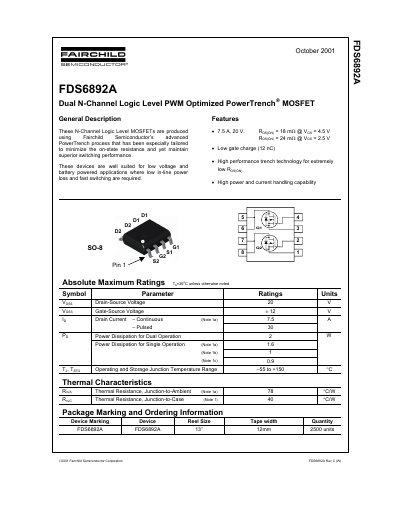
Fairchild Semiconductor FDS6892A Dual N-Channel MOSFET Datasheet
The FDS6892A is a dual N-channel logic level MOSFET produced using Fairchild Semiconductor's advanced PowerTrench process. It is designed to minimize on-state resistance while maintaining superior switching performance, making it well-suited for low voltage and battery-powered applications.
Key features include a 75A current rating, low gate charge of 12 nC, and high power handling capability. The device operates with a drain-source voltage of 20V and a maximum junction temperature range of -55°C to +150°C.
Fairchild FDS6892A specifications
| Drain-Source Voltage | 20 V |
|---|---|
| Gate-Source Voltage | -12 V |
| Pulsed Drain Current | 30 A |
| Power Dissipation (Dual) | 2 W |
| Operating Junction Temperature | -55 to +150 °C |
| Gate Charge | 12 nC |
| On-Resistance (Typical) | 18 mΩ |
Source: Fairchild Semiconductor FDS6892A Dual N-Channel MOSFET Datasheet
All Fairchild FDS6892A documents by type
Ratings, dimensions and ordering codes, for selection and design work.
Questions answered in these manuals
What is the maximum drain-source voltage?
The maximum drain-source voltage is 20 V.
From: Fairchild Semiconductor FDS6892A Dual N-Channel MOSFET Datasheet
What is the operating junction temperature range?
The operating and storage junction temperature range is -55 to +150 °C.
From: Fairchild Semiconductor FDS6892A Dual N-Channel MOSFET Datasheet
What is the maximum drain-source voltage for the FDS6892AZ?
20 V.
From: Fairchild FDS6892AZ Dual N-Channel Logic Level PWM Optimized PowerTrench® MOSFET Datasheet
What is the typical gate charge of the FDS6892AZ?
12 nC.
From: Fairchild FDS6892AZ Dual N-Channel Logic Level PWM Optimized PowerTrench® MOSFET Datasheet