
Key facts
- Brand
- Analog Devices
- Model
- AD7575
- Industry
- Industrial
- Documents
- 3
- Languages
- EN
- Last added
- 2012-08-02
Start here
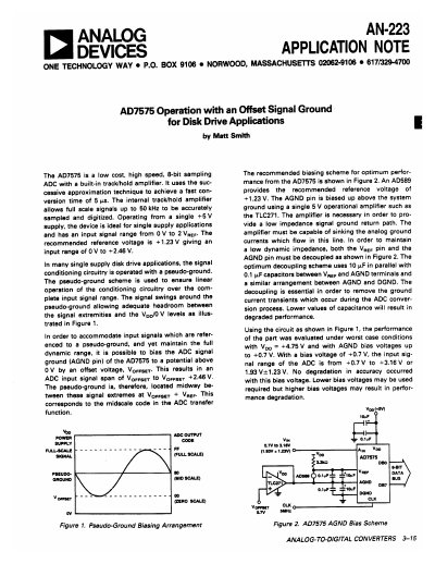
Analog Devices AN-223 Application Note AD7575 Operation with Offset Signal Ground
The document explains a biasing scheme for the AD7575 Analog-to-Digital Converter (ADC) to accommodate input signals referenced to a pseudo-ground. This setup ensures linear operation of the signal conditioning circuitry over the complete input signal range by biasing the ADC's analog ground (AGND) pin above system ground.
Read onlineAnalog Devices AD7575 specifications
| Resolution | 8 bits |
|---|---|
| Conversion Time (external clock) | 5 ms |
| Supply Voltage | +5 V |
| Reference Voltage | 1.23 V |
| Power Dissipation | 15 mW typ |
| Input Voltage Range | 0 to 2 VREF |
All Analog Devices AD7575 documents by type
Ratings, dimensions and ordering codes, for selection and design work.
How to use the product for one specific task, with worked examples.
Questions answered in these manuals
What is the maximum conversion time for the AD7575?
The device achieves a fast conversion time of 5 us.
From: Analog Devices AN-223 Application Note AD7575 Operation with Offset Signal Ground
What is the recommended reference voltage for the AD7575?
The recommended reference voltage is +1.23V.
From: Analog Devices AN-223 Application Note AD7575 Operation with Offset Signal Ground
What is the conversion time of the AD7575?
The AD7575 converts an input in 5 ms when using an external 4 MHz clock.
What supply voltage does the AD7575 require?
It operates from a single +5 V supply together with a 1.23 V band‑gap reference.
What is the conversion time of the AD7575?
The AD7575 has a fast conversion time of 5 ps.
What supply voltage does the AD7575 require?
It operates from a single +5 V supply.