
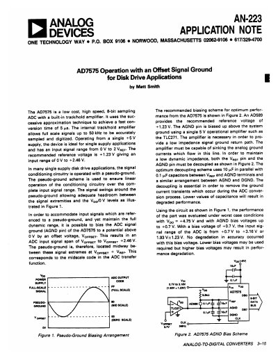
Analog Devices AN-223 Application Note AD7575 Operation with Offset Signal Ground


Analog Devices AN-223 Application Note AD7575 Operation with Offset Signal Ground - cover page
Brand
Analog Devices
Document type
Application Note
Language
English
Pages
1
File format
PDF
File size
63 KB
Published
02 August, 2012
Updated
29 August, 2012
Model
AD7575
MD5 checksum
FB73514DE8D02D6D08ACD1C30BF77524

About this manual

The document explains a biasing scheme for the AD7575 Analog-to-Digital Converter (ADC) to accommodate input signals referenced to a pseudo-ground. This setup ensures linear operation of the signal conditioning circuitry over the complete input signal range by biasing the ADC's analog ground (AGND) pin above system ground.

What's inside

  • Pseudo-Ground Biasing Arrangement
  • AD7575 AGND Bias Scheme
  • Recommended Reference Voltage
  • Decoupling Scheme
  • Performance Evaluation

Frequently asked questions

What is the maximum conversion time for the AD7575?

The device achieves a fast conversion time of 5 us.

What is the recommended reference voltage for the AD7575?

The recommended reference voltage is +1.23V.

What is the input signal range when using the recommended reference voltage?

The input range is from 0 V to +2.46 V.

Download PDF (63 KB)

More Analog Devices Manuals


View all Analog Devices manuals →