
Key facts
- Brand
- Fairchild
- Model
- FQA9P25
- Industry
- Industrial
- Documents
- 3
- Languages
- EN
- Last added
- 2012-07-12
Start here
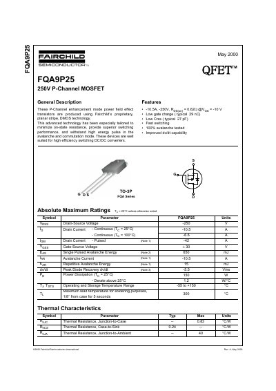
Fairchild Semiconductor FQA9P25 250V P-Channel MOSFET Datasheet
The FQA9P25 is a P-Channel enhancement mode power field effect transistor produced using Fairchild's proprietary planar stripe, DMOS technology. It is designed to minimize on-state resistance and provide superior switching performance, making it well-suited for high efficiency switching DC/DC converters.
The device features a maximum continuous drain current of -10.5A at 25°C and a drain-source breakdown voltage of -250V. It includes a built-in body diode with a maximum forward voltage of -5.0V and offers a thermal resistance of 0.83 °C/W from junction to case. The component is packaged in a TO-3P package.
Fairchild FQA9P25 specifications
| Drain-Source Voltage | -250 V |
|---|---|
| Continuous Drain Current (Tj = 25°C) | -10.5 A |
| Package Type | TO-3P |
| Power Dissipation (Tc = 25°C) | 150 W |
| Operating Temperature Range | -55 to +150 °C |
Source: Fairchild Semiconductor FQA9P25 250V P-Channel MOSFET Datasheet
All Fairchild FQA9P25 documents by type
Ratings, dimensions and ordering codes, for selection and design work.
Questions answered in these manuals
What is the operating and storage temperature range for this device?
The operating and storage temperature range is from -55 to +150 °C.
From: Fairchild Semiconductor FQA9P25 250V P-Channel MOSFET Datasheet
What is the maximum drain‑source voltage rating for the FQA9P25?
The device is rated for a maximum drain‑source voltage of -250 V.
What is the typical on‑resistance of the FQA9P25 at V_GS = -10 V?
The on‑resistance is 0.62 Ω when V_GS is -10 V.
What is the maximum continuous drain current of the FQA9P25?
The FQA9P25 can handle a continuous drain current of -10.5 A at 25 °C.
What is the typical gate charge of the FQA9P25?
The typical gate charge is 29 nC.