
This datasheet provides information about the FQA9P25 device parameters, including pin definitions, package, ratings, and characteristics. It can be used to understand the performance of the device.
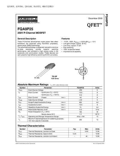
The FQA9P25 is a P‑Channel enhancement mode power MOSFET built with Fairchild's planar stripe DMOS technology. It is designed for high‑efficiency switching DC/DC converters, offering low gate charge and low output capacitance for fast switching performance.
Key specifications include a -250 V drain‑source rating, -10.5 A continuous drain current, typical on‑resistance of 0.62 Ω at VGS = ‑10 V, and a single‑pulse avalanche energy of 650 mJ. The device is supplied in a TO‑3P package with thermal resistance values suitable for high‑power applications.
| Drain‑Source Voltage (V_DSS) | -250 V |
|---|---|
| Continuous Drain Current (I_D) at 25 °C | -10.5 A |
| On‑Resistance (R_DS(on)) typical | 0.62 Ω @ V_GS = -10 V |
| Typical Gate Charge (Q_g) | 29 nC |
| Power Dissipation (P_D) at 25 °C | 150 W |
| Junction‑to‑Case Thermal Resistance (RθJC) | 0.83 °C/W |
The FQA9P25 can handle a continuous drain current of -10.5 A at 25 °C.
The typical gate charge is 29 nC.
The device is rated for a single‑pulse avalanche energy of 650 mJ.