
Key facts
- Brand
- STMicroelectronics
- Model
- VNS3NV04D
- Category
- Other Electronics
- Documents
- 3
- Languages
- EN
- Last added
- 2012-08-08
Start here
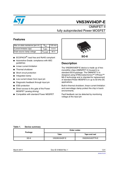
STMicroelectronics VNS3NV04DP-E OMNIFET II Datasheet
The VNS3NV04DP-E is an OMNIFET II device consisting of two monolithic chips housed in a standard SO-8 package. It is designed for use in up to 50 kHz DC applications as a replacement for standard Power MOSFETs. The device integrates built-in protection features including overvoltage clamping, linear current limitation, and thermal shutdown to operate safely in harsh environments.
Read onlineSTMicroelectronics VNS3NV04D specifications
| Max on-state resistance (per channel) | 120 mΩ |
|---|---|
| Current limitation (typical) | 3.5 A |
| Drain-source clamp voltage | 40 V |
| Operating junction temperature | Internally limited |
| Storage temperature | -55 to 150 °C |
Source: STMicroelectronics VNS3NV04DP-E OMNIFET II Datasheet
All STMicroelectronics VNS3NV04D documents by type
Ratings, dimensions and ordering codes, for selection and design work.
Questions answered in these manuals
What is the typical current limitation of the VNS3NV04DP-E?
The typical current limitation is 3.5 A.
Is the VNS3NV04DP-E RoHS compliant?
Yes, it is ECOPACK compliant, meaning it is lead free and RoHS compliant.
What is the maximum On-State resistance per channel?
The maximum On-State resistance per channel is 120 mΩ.
What is the typical current limitation?
The typical current limitation is 3.5 A.
What is the overtemperature shutdown threshold?
The device shuts down when the junction temperature reaches between 150 and 200 °C, with a typical value of 175 °C.
From: STMicroelectronics VNS3NV04D OMNIFET II Power MOSFET Datasheet
Is there ESD protection?
Yes, the device includes ESD protection according to the Human Body model.
From: STMicroelectronics VNS3NV04D OMNIFET II Power MOSFET Datasheet