
Key facts
- Brand
- STMicroelectronics
- Model
- VNS1NV04D
- Category
- Other Electronics
- Documents
- 2
- Languages
- EN
- Last added
- 2012-08-08
Start here
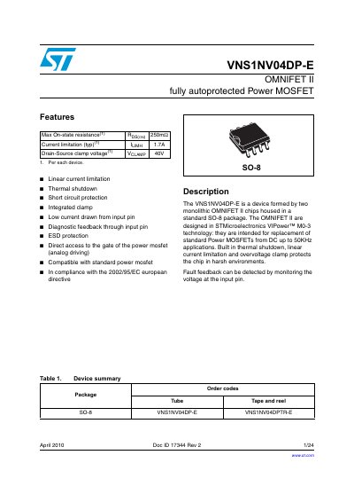
STMicroelectronics VNS1NV04DP-E OMNIFET II Datasheet
The VNS1NV04DP-E is an OMNIFET II device formed by two monolithic chips housed in a standard SO-8 package. It is designed for replacement of standard Power MOSFETs from DC up to 50KHz, offering built-in protection features such as thermal shutdown, linear current limitation, and overvoltage clamp.
The document provides detailed electrical specifications including absolute maximum ratings, thermal data, and dynamic characteristics like switching times and capacitance. It also covers protection mechanisms for overtemperature, short circuits, and fault feedback monitoring.
STMicroelectronics VNS1NV04D specifications
| Drain-source clamp voltage (typ) | 40 V |
|---|---|
| Current limitation (typ) | 1.7 A |
| Operating junction temperature range | -55 to 150 °C |
| Total dissipation at Tj = 25 °C | 4 W |
Source: STMicroelectronics VNS1NV04DP-E OMNIFET II Datasheet
All STMicroelectronics VNS1NV04D documents by type
Ratings, dimensions and ordering codes, for selection and design work.
Questions answered in these manuals
What is the maximum operating junction temperature?
The device has an internally limited operating junction temperature, with a storage temperature range of -55 to 150 °C.
What is the typical current limitation value?
The typical current limitation is 1.7 A, with a maximum of 3.5 A under specific test conditions.
What is the maximum operating frequency for the VNS1NV04D?
The device is intended for replacement of standard Power MOSFETs from DC up to 50KHz applications.
How does the device indicate a fault condition?
In the case of an overtemperature fault, the device tries to sink a diagnostic current through the INPUT pin to indicate the condition.