
Key facts
- Brand
- Infineon
- Model
- SPB20N60S5
- Industry
- Industrial
- Documents
- 3
- Languages
- EN
- Last added
- 2012-04-06
Start here
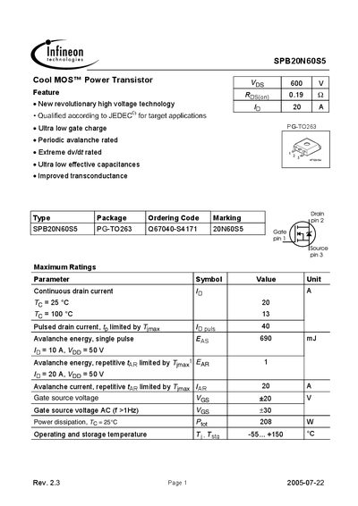
Infineon SPB20N60S5 Datasheet
The SPB20N60S5 is a Cool MOS™ power transistor featuring ultra‑low gate charge, high voltage capability, and robust avalanche performance. It is supplied in a PG‑TO263 package and qualified according to JEDEC for target applications.
The document provides maximum ratings, thermal characteristics, electrical parameters, gate‑charge data, and typical output characteristics, along with mechanical footprint dimensions and safety notices.
Infineon SPB20N60S5 specifications
| Continuous drain current (ID) at 25 °C | 20 A |
|---|---|
| Avalanche energy (single pulse) | 690 mJ |
| Power dissipation at 25 °C (PD) | 208 W |
Source: Infineon SPB20N60S5 Datasheet
All Infineon SPB20N60S5 documents by type
Ratings, dimensions and ordering codes, for selection and design work.
Questions answered in these manuals
What is the maximum continuous drain current of the SPB20N60S5?
The device can conduct up to 20 A continuously at an ambient temperature of 25 °C.
How much power can the transistor dissipate at 25 °C?
It is rated for a power dissipation of 208 W at a case temperature of 25 °C.
What is the maximum drain‑source voltage of the SPP20N60S5?
The device is rated for a drain‑source breakdown voltage of 600 V.
From: infineon SPP20N60S5 Preliminary data SPB20N60S5 Manual
How much continuous drain current can the SPP20N60S5 handle at 25 °C?
It can conduct up to 20 A continuously at 25 °C.
From: infineon SPP20N60S5 Preliminary data SPB20N60S5 Manual
What is the maximum continuous drain current?
The device can conduct up to 20 A continuously at a case temperature of 25 °C.
From: Infineon SPP20N60S5 / SPB20N60S5 Power MOSFET Datasheet
What is the allowed gate‑source voltage?
The maximum gate‑source voltage is +20 V.
From: Infineon SPP20N60S5 / SPB20N60S5 Power MOSFET Datasheet