
Key facts
- Brand
- Infineon
- Model
- TLE 6266 G
- Category
- Automotive supplies
- Documents
- 2
- Languages
- EN
- Last added
- 2012-04-05
Start here
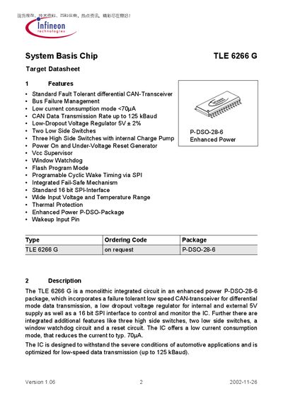
Infineon TLE 6266 G System Basis Chip Datasheet
The TLE 6266 G is a monolithic System Basis Chip designed for automotive applications. It integrates a fault‑tolerant low‑speed CAN‑transceiver, a low‑dropout 5 V regulator, three high‑side switches, two low‑side switches, a window watchdog, and a 16‑bit SPI interface for control and monitoring.
The device offers four operation modes—normal, receive‑only, Vbat stand‑by and cyclic wake—selected via SPI bits. Detailed pin definitions, functional block diagrams and circuit descriptions are provided to aid designers in implementing the chip in safety‑critical systems.
Infineon TLE 6266 G specifications
| CAN data transmission rate | 125 kBaud |
|---|---|
| Low‑current consumption mode | 70 µA (typ.) |
| Low‑dropout voltage regulator | 5 V ±2 % |
| Low side switches | 2 |
| High side switches | 3 with internal charge pump |
| Window watchdog | Enabled |
| Fail‑safe mechanism | Integrated |
| Input voltage and temperature range | Wide |
All Infineon TLE 6266 G documents by type
Ratings, dimensions and ordering codes, for selection and design work.
Questions answered in these manuals
What is the maximum CAN data transmission rate of the TLE 6266 G?
The chip supports a CAN data rate of up to 125 kBaud.
How many high side switches are integrated in the TLE 6266 G?
It contains three high side switches with an internal charge pump.
What is the maximum CAN data rate of the TLE 6266 G?
The chip supports a CAN data transmission rate of up to 125 kBaud.
How many high‑side switches are integrated in the TLE 6266 G?
It contains three high‑side switches with an internal charge pump.