
Key facts
- Brand
- Analog Devices
- Model
- AD1890
- Industry
- Industrial
- Documents
- 4
- Languages
- EN
- Last added
- 2022-09-14
Start here
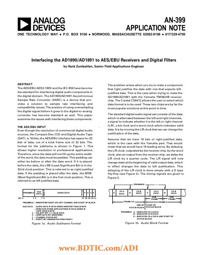
Analog Devices AD1890/AD1891 Application Note
The document addresses compatibility issues when interfacing the AD1890/AD1891 Asynchronous Sample Rate Converter (ASRC) with components that use different data justification formats, such as the Yamaha YM3623B receiver chip and the NPC SM5813 digital filter. It details the AES/EBU input format, explaining the difference between right-justified and left-justified data within the 32-bit frame structure.
Read onlineAnalog Devices AD1890 specifications
| Dynamic Range (AD1890) | 120 dB |
|---|---|
| Dynamic Range (AD1891) | 96 dB |
| Supply Voltage (VDD) | 2.7 V – 5.5 V |
| Supply Current (VDD = 5.0 V) | 35 mA – 40 mA |
| Sample Clock Frequency Range | 8 kHz – 56 kHz |
| Clock Ratio | 1:2 – 2:1 |
| Input Word Width (AD1890) | 4 – 20 bits |
Source: Analog Devices AD1890/AD1891 SamplePort Stereo Asynchronous Sample Rate Converter Datasheet
All Analog Devices AD1890 documents by type
Ratings, dimensions and ordering codes, for selection and design work.
How to use the product for one specific task, with worked examples.
Questions answered in these manuals
What is the difference between right-justified and left-justified data in AES/EBU?
Right-justified data places the LSB in the 32nd clock position, while left-justified data places the MSB in the first clock position.
How can data justification be changed for the Yamaha YM3623B?
By delaying the L/R clock output by the word clock using a D type flip-flop, the data format changes from right-justified to left-justified.
What is the standard for interfacing digital audio components in the digital domain?
The AES/EBU AES3-199X and the IEC-958 have become the standard for interfacing digital audio components in the digital domain.
From: Analog Devices AN-399 Interfacing AD1890/AD1891 to AES Receivers
How can data justification be changed from right-justified to left-justified?
Data justification can be changed by delaying the L/R clock outputted by the receiver chip by the word clock, effectively changing the data to left justification.
From: Analog Devices AN-399 Interfacing AD1890/AD1891 to AES Receivers
What is the supply voltage range for the AD1890/AD1891?
The devices operate from a VDD of 2.7 V to 5.5 V.
From: Analog Devices AD1890/AD1891 SamplePort Stereo Asynchronous Sample Rate Converter Datasheet
How much sample‑clock jitter can the AD1890/AD1891 tolerate?
The input and output sample‑clock jitter tolerance is up to 10 ns for less than 1 dB degradation in THD+N.
From: Analog Devices AD1890/AD1891 SamplePort Stereo Asynchronous Sample Rate Converter Datasheet