
This document discusses the interface issues and compatibility of the AD1890/AD1891 Asynchronous Sample Rate Converter (ASRC), as well as the standardization of oversampling the digital signal before it goes to the digital-to-analog converter. The document also introduces the format of the AES/EBU interface and the data padding method.
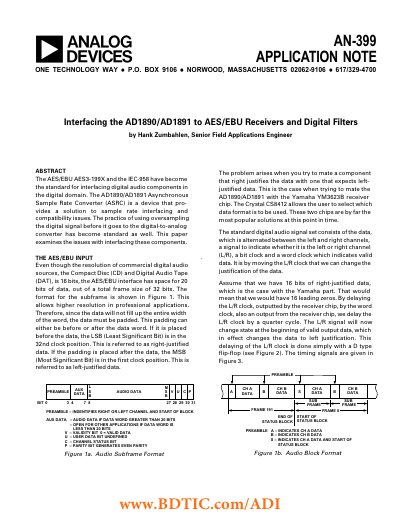
The document addresses compatibility issues when interfacing the AD1890/AD1891 Asynchronous Sample Rate Converter (ASRC) with components that use different data justification formats, such as the Yamaha YM3623B receiver chip and the NPC SM5813 digital filter. It details the AES/EBU input format, explaining the difference between right-justified and left-justified data within the 32-bit frame structure.
Right-justified data places the LSB in the 32nd clock position, while left-justified data places the MSB in the first clock position.
By delaying the L/R clock output by the word clock using a D type flip-flop, the data format changes from right-justified to left-justified.
The L/R clock is delayed by the word clock to change the justification from left-justified to right-justified, matching the filter's expectation.