
Key facts
- Brand
- Analog Devices
- Model
- ADN2814
- Industry
- Industrial
- Documents
- 3
- Languages
- EN
- Last added
- 2012-06-08
Start here
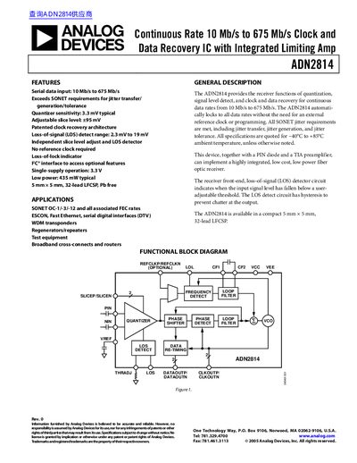
Analog Devices ADN2814 Data Recovery IC Datasheet
The ADN2814 is a continuous rate clock and data recovery integrated circuit designed for data rates from 10 Mb/s to 675 Mb/s. It features an integrated limiting amplifier and quantizer, meeting SONET requirements for jitter transfer, generation, and tolerance. The device operates with a single 3.3 V supply and requires no external reference clock.
Read onlineAnalog Devices ADN2814 specifications
| Data Rate | 10 Mb/s to 675 Mb/s |
|---|---|
| Supply Voltage | 3.3 V |
| Operating Temperature | -40°C to +85°C |
| Package | 5mm x 5mm, 32-lead LFCSP |
| Power Consumption | 435 mW typical |
All Analog Devices ADN2814 documents by type
Ratings, dimensions and ordering codes, for selection and design work.
Questions answered in these manuals
Does the ADN2814 require a reference clock?
No, the device automatically locks to all data rates without the need for an external reference clock or programming.
What is the loss-of-signal detect range?
The loss-of-signal detect range is 2.3 mV to 19 mV.
What data rates does the ADN2814 support?
The ADN2814 operates from 10 Mb/s up to 675 Mb/s.
From: Analog Devices ADN2814 Clock and Data Recovery IC Datasheet
What is the recommended supply voltage for the ADN2814?
The device is specified for a 3.0 V to 3.6 V supply, with 3.3 V typical.
From: Analog Devices ADN2814 Clock and Data Recovery IC Datasheet
What data rates does the ADN2814 support?
The device supports continuous data rates from 10 Mb/s up to 675 Mb/s.
Is an external reference clock required for the ADN2814?
No, the ADN2814 automatically locks to the data rate without an external reference clock.