
ADN2814 is a clock and data recovery integrated circuit from Analog Devices that can be used for 10 Mb/s to 675 Mb/s continuous rate data, has an adjustable slice level, independent slice level adjustment and loss of signal detector, does not require a reference clock, and has low power consumption and Pb free packaging.
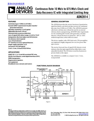
The ADN2814 is a continuous rate clock and data recovery integrated circuit designed for data rates from 10 Mb/s to 675 Mb/s. It features an integrated limiting amplifier and quantizer, meeting SONET requirements for jitter transfer, generation, and tolerance. The device operates with a single 3.3 V supply and requires no external reference clock.
| Data Rate | 10 Mb/s to 675 Mb/s |
|---|---|
| Supply Voltage | 3.3 V |
| Operating Temperature | -40°C to +85°C |
| Package | 5mm x 5mm, 32-lead LFCSP |
| Power Consumption | 435 mW typical |
No, the device automatically locks to all data rates without the need for an external reference clock or programming.
The loss-of-signal detect range is 2.3 mV to 19 mV.
Yes, it meets all SONET requirements for jitter transfer, jitter generation, and jitter tolerance.