
ADN2814 is a clock and data recovery IC from Analog Devices that supports 10 Mb/s to 675 Mb/s continuous rates and integrates a limiting amplifier.
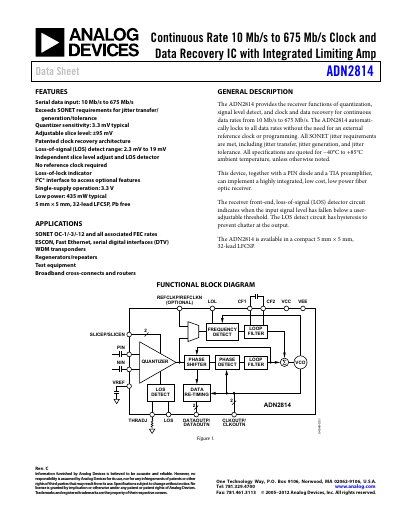
The ADN2814 is a continuous‑rate clock and data recovery integrated circuit that operates from 10 Mb/s to 675 Mb/s without an external reference clock. It includes a built‑in limiting amplifier, loss‑of‑signal detection, and an I²C interface for optional features. The device meets SONET jitter requirements and is supplied in a 5 mm × 5 mm 32‑lead LFCSP package.
The datasheet contains sections on features, applications, functional block diagram, detailed electrical specifications, jitter performance, output and timing characteristics, pin configuration, I²C interface timing, thermal data, and ordering information. Designers can use the provided PCB guidelines and typical performance curves to integrate the ADN2814 into fiber‑optic receivers, transponders, and high‑speed serial links.
| Data Rate | 10 Mb/s to 675 Mb/s |
|---|---|
| Power Supply Voltage | 3.0 V – 3.6 V (typical 3.3 V) |
| Power Consumption (locked) | 435 mW typical |
| Package | 5 mm × 5 mm, 32‑lead LFCSP |
| Operating Temperature Range | –40 °C to +85 °C |
| Input Voltage Range (PIN/NIN) | 1.8 V – 2.8 V |
| I²C Clock Frequency | 400 kHz |
The ADN2814 operates from 10 Mb/s up to 675 Mb/s.
The device is specified for a 3.0 V to 3.6 V supply, with 3.3 V typical.
It is offered in a 5 mm × 5 mm, 32‑lead LFCSP package.