
Key facts
- Brand
- Analog Devices
- Model
- ADG333A
- Industry
- Industrial
- Documents
- 3
- Languages
- EN
- Last added
- 2012-06-08
Start here
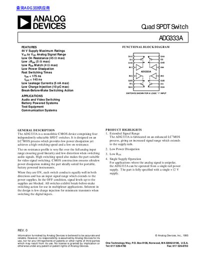
Analog Devices ADG333A Quad SPDT Switch Datasheet
The ADG333A is a monolithic CMOS device comprising four independently selectable SPDT switches. It is designed on an LC-MOS process which provides low power dissipation yet achieves a high switching speed and a low on resistance. The on resistance profile is very flat over the full analog input range ensuring good linearity and low distortion when switching audio signals.
The device features low leakage currents (5 nA max) and low charge injection (10 pC max). It exhibits break-before-make switching action for use in multiplexer applications. The ADG333A is ideally suited for portable, battery powered instruments due to its CMOS construction.
Analog Devices ADG333A specifications
| Number of Switches | 4 |
|---|---|
| Maximum Supply Voltage | 44 V |
| Maximum On Resistance | 45 Ω |
| Maximum Leakage Current | 5 nA |
| Maximum Charge Injection | 10 pC |
| Maximum Turn-On Time | 175 ns |
All Analog Devices ADG333A documents by type
Ratings, dimensions and ordering codes, for selection and design work.
Questions answered in these manuals
What are the applications for the ADG333A?
The ADG333A is suitable for audio and video switching, battery powered systems, test equipment, and communication systems.
Does the ADG333A support single supply operation?
Yes, the part is fully specified with a single +12 V supply for applications where the analog signal is unipolar.
What is the typical on‑resistance of the ADG333A?
The typical on‑resistance is 20 Ω.
How should the power supplies be sequenced when powering the ADG333A?
First apply Vpp, then Vss, and finally the logic signals.
What is the maximum voltage difference allowed between Vop and Vss?
The maximum Vop‑to‑Vss voltage is +44 V.
How should the power supplies be sequenced when powering the ADG333A?
Turn on Vop first, then Vss, and finally the logic signals.