
Key facts
- Brand
- Agilent
- Model
- HSMS-282x
- Category
- Other Electronics
- Documents
- 2
- Languages
- EN
- Last added
- 2012-06-05
Start here
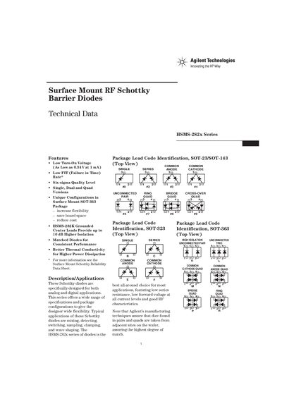
Agilent HSMS-282x Series Surface Mount RF Schottky Barrier Diodes Technical Data
This document provides technical specifications and application information for the Agilent HSMS-282x family of Surface Mount RF Schottky Barrier Diodes. These devices are designed for both analog and digital applications, including mixing, detecting, switching, sampling, clamping, and wave shaping.
The series offers single, dual, and quad versions in unique SOT-363 packages to increase flexibility and save board space. Key features include a low turn-on voltage as low as 0.34 V at 1 mA, a six-sigma quality level, and matched diodes for consistent performance.
Agilent HSMS-282x specifications
| Forward Current (1 us Pulse) | 1 Amp |
|---|---|
| Peak Inverse Voltage | 15 V |
| Junction Temperature | 150 °C |
| Storage Temperature | -65 to 150 °C |
| Thermal Resistance (SOT-23/SOT-143) | 500 °C/W |
| Thermal Resistance (SOT-323/SOT-363) | 150 °C/W |
| Effective Carrier Lifetime | 100 ps maximum |
Source: Agilent HSMS-282x Series Surface Mount RF Schottky Barrier Diodes Technical Data
All Agilent HSMS-282x documents by type
Ratings, dimensions and ordering codes, for selection and design work.
Questions answered in these manuals
What are the typical applications of HSMS-282x Schottky diodes?
Typical applications include mixing, detecting, switching, sampling, clamping, and wave shaping.
From: Agilent HSMS-282x Series Surface Mount RF Schottky Barrier Diodes Technical Data
What is the low turn-on voltage for this series?
The turn-on voltage can be as low as 0.34 V at 1 mA.
From: Agilent HSMS-282x Series Surface Mount RF Schottky Barrier Diodes Technical Data
What is the maximum forward current rating for the HSMS-282x diodes?
The diodes are rated for a 1 µs pulse forward current of 1 A.
How does Agilent ensure diode matching in paired or quad configurations?
Dice for pairs and quads are taken from adjacent sites on the wafer to achieve the highest degree of match.