
Key facts
- Brand
- Infineon
- Model
- TDA21201
- Documents
- 2
- Languages
- EN
- Last added
- 2012-04-01
Start here
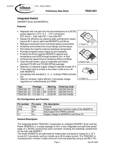
Infineon TDA21201 Integrated Switch Preliminary Data Sheet
The Integrated Switch TDA21201 combines a MOSFET driver, a high‑side MOSFET and a low‑side MOSFET in one TO‑220 or TO‑263 package, enabling a compact, efficient power stage for 12 V to sub‑3.3 V DC‑DC converters. It eliminates external bootstrap components and reduces part count, board space, and design complexity.
The document lists absolute maximum ratings, thermal characteristics, electrical parameters, and layout recommendations, and includes typical application circuits for multi‑phase converters, shutdown operation, and current‑sense methods.
Infineon TDA21201 specifications
| Maximum DC output current | 30 A |
|---|---|
| Junction temperature (max) | 150 °C |
| Thermal resistance, junction‑case | 1.9 K/W |
| Supply voltage range (VCC) | 9 V to 15 V |
| Input signal transition frequency | 100 kHz to 500 kHz |
| Power dissipation | 10 W |
Source: Infineon TDA21201 Integrated Switch Preliminary Data Sheet
All Infineon TDA21201 documents by type
Ratings, dimensions and ordering codes, for selection and design work.
Questions answered in these manuals
What is the maximum output current of the TDA21201?
The device can deliver up to 30 A of DC output current at a 12 V supply.
From: Infineon TDA21201 Integrated Switch Preliminary Data Sheet
What temperature range can the TDA21201 operate in?
It is rated for junction temperatures from –25 °C up to 125 °C, with a shutdown at 150 °C.
From: Infineon TDA21201 Integrated Switch Preliminary Data Sheet
What input voltage range can the device operate from?
It operates with a supply voltage (VCC) between 9 V and 15 V.