
Key facts
- Brand
- Analog Devices
- Model
- ADA4899-1
- Industry
- Industrial
- Documents
- 4
- Languages
- EN
- Last added
- 2012-06-08
Start here
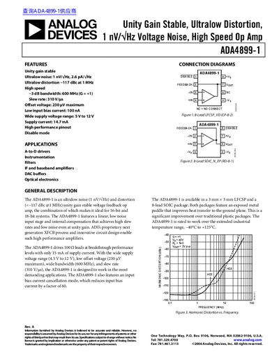
Analog Devices ADA4899-1 Op Amp Datasheet
The ADA4899-1 is a high-performance voltage feedback operational amplifier designed for demanding applications requiring ultralow noise and distortion. It features a unity gain stable architecture with an ultralow input voltage noise of 1 nV/√Hz and an ultralow harmonic distortion of -117 dBc at 1 MHz. The device is ideal for 16-bit and 18-bit systems, serving as an A-to-D driver, instrumentation amplifier, or filter component.
Read onlineAnalog Devices ADA4899-1 specifications
| Input Voltage Noise | 1.0 nV/√Hz |
|---|---|
| Harmonic Distortion | -117 dBc at 1 MHz |
| -3 dB Bandwidth | 600 MHz |
| Slew Rate | 310 V/μs |
| Input Offset Voltage | 230 pV maximum |
| Input Bias Current | 100 nA |
| Supply Voltage Range | 5 V to 12 V |
| Supply Current | 14.7 mA |
| Operating Temperature Range | -40°C to +125°C |
All Analog Devices ADA4899-1 documents by type
Ratings, dimensions and ordering codes, for selection and design work.
Day-to-day operation, settings and troubleshooting. Start here if the product is already set up.
Questions answered in these manuals
What is the input voltage noise of the ADA4899-1?
The input voltage noise is 1.0 nV/√Hz at 100 kHz.
What is the harmonic distortion at 1 MHz?
The harmonic distortion is -117 dBc at 1 MHz.
What is the unity‑gain bandwidth of the ADA4899‑1?
The op‑amp has a 3‑dB bandwidth of 600 MHz at unity gain.
How much supply current does the ADA4899‑1 draw in normal operation?
It draws a typical quiescent supply current of 14.7 mA.
What temperature range can the ADA4899-1 operate in?
It is rated for –40 °C to +125 °C operation.
Which package types are offered for the ADA4899-1?
It is available in a 3 mm × 3 mm LFCSP and an 8‑lead SOIC package.