
Key facts
- Brand
- Texas Instruments
- Model
- CD4012B
- Industry
- Industrial
- Documents
- 2
- Languages
- EN
- Last added
- 2012-06-06
Start here
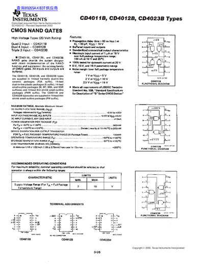
Texas Instruments CD4011B/CD4012B/CD4023B CMOS NAND Gates Datasheet
The document details the CD4011B, CD4012B, and CD4023B types of CMOS NAND gates. These devices are supplied in various 14-lead packages, including hermetic dual-in-line ceramic (F3A_ suffix), plastic (E suffix), small-outline (M, MT, M96, NSR suffixes), and thin shrink small-outline (PWR or PW suffix) options.
Key specifications include a propagation delay time of 60 ns typical at CL = 50 pF and Vop = 10 V. The devices feature buffered inputs and outputs with standardized symmetrical output characteristics, meeting JEDEC Tentative Standard No. 13B requirements.
All Texas Instruments CD4012B documents by type
Ratings, dimensions and ordering codes, for selection and design work.
Questions answered in these manuals
Are the inputs and outputs buffered?
Yes, all inputs and outputs are buffered.
From: Texas Instruments CD4011B/CD4012B/CD4023B CMOS NAND Gates Datasheet
What is the maximum supply voltage for these NAND gates?
The devices can operate with a DC supply voltage ranging from -0.5V to +20V.
From: Texas Instruments CD4011B/CD4012B/CD4023B CMOS NAND Gates Datasheet
What is the propagation delay time of the CD4011B/ CD4012B/ CD4023B devices?
The typical propagation delay is 60 ns when the load capacitance is 50 pF and the supply voltage is 10 V.
What supply voltage range do these NAND gates support?
They operate from 0.5 V up to 20 V.