
Key facts
- Brand
- Texas Instruments
- Model
- SN74LVC541
- Category
- Other Electronics
- Industry
- Electronics
- Documents
- 2
- Languages
- EN
- Last added
- 2012-05-09
Start here
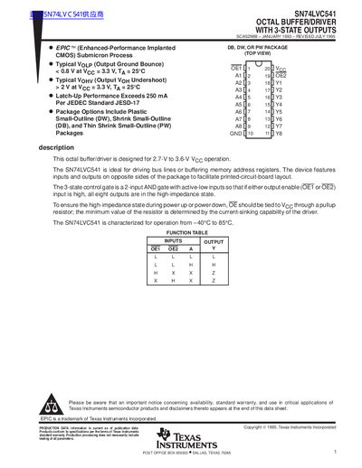
Texas Instruments SN74LVC541 Octal Buffer/Driver Datasheet
The SN74LVC541 octal buffer/driver provides 3‑state outputs and is intended for 2.7‑V to 3.6‑V VCC operation. It is suited for driving bus lines or buffering memory address registers, with inputs and outputs on opposite sides of the package to aid PCB layout. The 3‑state control gate uses a 2‑input AND with active‑low inputs, allowing all outputs to enter high‑impedance when either OE pin is high.
The device is available in multiple plastic packages (DW, DB, PW) and is characterized for –40 °C to 85 °C operation. Electrical specifications include supply voltage range, input thresholds, output current capabilities, and timing parameters. An important notice about warranty, availability, and critical‑application use appears at the end of the sheet.
Texas Instruments SN74LVC541 specifications
| Supply voltage (SN54LVC541A) | 2.7 V to 3.6 V VCC |
|---|---|
| Supply voltage (SN74LVC541A) | 1.65 V to 3.6 V VCC |
| Typical propagation delay | 5.1 ns at 3.3 V |
| Output current capability | Up to 250 mA per pin |
| ESD protection | 2000 V Human‑Body Model, 200 V Machine Model, 1000 V Charged‑Device Model |
Source: TEXAS INSTRUMENTS SN54LVC541A SN74LVC541A OCTAL BUFFERS/DRIVERS WITH 3-STATE OUTPUTS Manual
All Texas Instruments SN74LVC541 documents by type
Ratings, dimensions and ordering codes, for selection and design work.
Questions answered in these manuals
What temperature range can the SN74LVC541 operate in?
It is specified for operation from –40 °C to 85 °C.
From: Texas Instruments SN74LVC541 Octal Buffer/Driver Datasheet
What is the function of the 3‑state control gate?
It is a 2‑input AND gate with active‑low inputs; if either output‑enable input is high, all eight outputs go to high‑impedance.
From: TEXAS INSTRUMENTS SN54LVC541A SN74LVC541A OCTAL BUFFERS/DRIVERS WITH 3-STATE OUTPUTS Manual
How should the output‑enable pin be biased during power‑up or power‑down?
Tie OE to VCC through a pull‑up resistor; the resistor value must be chosen based on the driver’s current‑sinking capability.
From: TEXAS INSTRUMENTS SN54LVC541A SN74LVC541A OCTAL BUFFERS/DRIVERS WITH 3-STATE OUTPUTS Manual