
This document is a PDF datasheet of CD4011B, CD4012B, and CD4023B types, including their packaging types, pin counts, package quantities, eco plan, lead/ball finish, MSL peak temperature, etc.
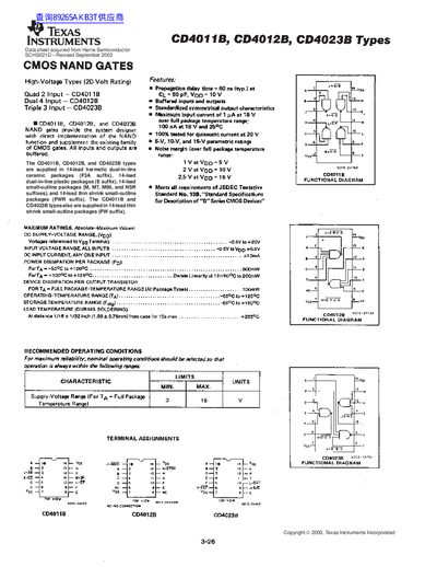
The document details the CD4011B, CD4012B, and CD4023B types of CMOS NAND gates. These devices are supplied in various 14-lead packages, including hermetic dual-in-line ceramic (F3A_ suffix), plastic (E suffix), small-outline (M, MT, M96, NSR suffixes), and thin shrink small-outline (PWR or PW suffix) options.
Key specifications include a propagation delay time of 60 ns typical at CL = 50 pF and Vop = 10 V. The devices feature buffered inputs and outputs with standardized symmetrical output characteristics, meeting JEDEC Tentative Standard No. 13B requirements.
| Propagation delay time (typ.) | 60 ns at CL = 50 pF, Vop = 10 V |
|---|
Yes, all inputs and outputs are buffered.
The devices can operate with a DC supply voltage ranging from -0.5V to +20V.
The propagation delay time is typically 60 ns when the load capacitance is 50 pF and the supply voltage is 10 V.