
Key facts
- Brand
- Texas Instruments
- Model
- SN74AC11
- Category
- Other Electronics
- Documents
- 2
- Languages
- EN
- Last added
- 2012-05-08
Start here
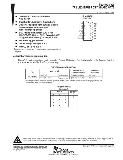
Texas Instruments SN74AC11-Q1 Datasheet
The SN74AC11-Q1 contains three independent 3‑input AND gates that implement the Boolean function Y = A·B·C in positive logic. It operates from 2 V to 6 V supply voltage, accepts input voltages up to VCC+0.5 V, and provides typical propagation delays of 7.5 ns at 5 V.
The device is offered in SOIC‑D and TSSOP‑PW packages, with mechanical drawings, thermal impedance data, and automotive‑grade qualifications (AEC‑Q100). Absolute‑maximum ratings, recommended operating conditions, and ESD protection exceeding 2000 V are documented, along with packaging status and RoHS compliance information.
Texas Instruments SN74AC11 specifications
| Supply voltage range | 2 V to 6 V |
|---|---|
| Maximum propagation delay | 7.5 ns at 5 V |
| Operating temperature range | -40 °C to 85 °C |
| ESD protection rating | Exceeds 2000 V |
All Texas Instruments SN74AC11 documents by type
Ratings, dimensions and ordering codes, for selection and design work.
Questions answered in these manuals
What is the supply voltage range for the SN74AC11‑Q1?
The device operates from 2 V to 6 V supply voltage.
What is the maximum propagation delay of the SN74AC11‑Q1?
The maximum propagation delay is 7.5 ns at a 5 V supply.
What are the recommended operating temperature ranges for these devices?
For PDIP, SOIC, and similar packages the range is –55 °C to 125 °C; for SSOP, TSSOP and other surface‑mount packages it is –40 °C to 85 °C.
From: Texas Instruments SN54AC11 SN74AC11 Triple 3-Input Positive-AND Gates Datasheet
Which package options are available for the SN74AC11?
Available packages include PDIP (N), SOIC (D), SSOP (DB), TSSOP (PW), CDIP (J), CFP (W), and LOCC (FK), each with corresponding part numbers.
From: Texas Instruments SN54AC11 SN74AC11 Triple 3-Input Positive-AND Gates Datasheet