
Key facts
- Brand
- Maxim
- Model
- MAX394
- Industry
- Industrial
- Documents
- 2
- Languages
- EN
- Last added
- 2012-06-07
Start here
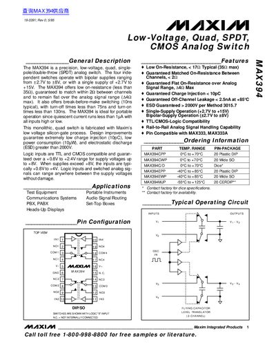
Maxim MAX394 Low-Voltage Quad SPDT CMOS Analog Switch Datasheet
The MAX394 is a precision, low-voltage, quad, single-pole/double-throw (SPDT) analog switch designed for portable operation. It features four independent switches that operate with bipolar supplies ranging from +2.7V to +8V or a single supply of +2.7V to +15V.
Key characteristics include low on-resistance (less than 35Ω), guaranteed matching within 2Ω between channels, and break-before-make switching. The device offers extremely low charge injection (10pC) and quiescent current less than 1pA.
Maxim MAX394 specifications
| On-Resistance (Max) | < 35Ω |
|---|---|
| On-Resistance Match Between Channels | < 2Ω |
| Charge Injection (Max) | < 10pC |
| Quiescent Current (Max) | < 1pA |
| ESD Rating | > 2000V |
| Logic Input Compatibility | TTL and CMOS |
Source: Maxim MAX394 Low-Voltage Quad SPDT CMOS Analog Switch Datasheet
All Maxim MAX394 documents by type
Ratings, dimensions and ordering codes, for selection and design work.
Questions answered in these manuals
What is the supply voltage range for bipolar operation?
The device operates with bipolar supplies ranging from +2.7V to +8V.
From: Maxim MAX394 Low-Voltage Quad SPDT CMOS Analog Switch Datasheet
What is the supply voltage range for single-supply operation?
It supports a single supply of +2.7V to +15V.
From: Maxim MAX394 Low-Voltage Quad SPDT CMOS Analog Switch Datasheet
What is the maximum single‑supply voltage for the MAX394?
The MAX394 can operate from a single supply of +2.7 V up to +15 V.
From: Maxim MAX394 Low-Voltage Quad SPDT CMOS Analog Switch Datasheet
What is the typical on‑resistance of the MAX394?
The typical on‑resistance is less than 35 Ω.
From: Maxim MAX394 Low-Voltage Quad SPDT CMOS Analog Switch Datasheet