
The document describes the features and characteristics of a product named TLE 6266 G, which is an enhanced power system basis chip. The chip features a standard fault tolerant differential CAN-transceiver, bus failure management, low current consumption mode, CAN data transmission rate up to 125 kBaud, low-dropout voltage regulator of 5V±2%, two low side switches, three high side switches with internal charge pump, power on and under-voltage reset generator, Vcc supervisor, window watchdog, flash program mode, programable cyclic wake timing via SPI, integrated fail-safe mechanism, standard 16 bit SPI-interface, wide input voltage and temperature range, thermal protection, enhanced power P-DSO-package, and wakeup input pin.
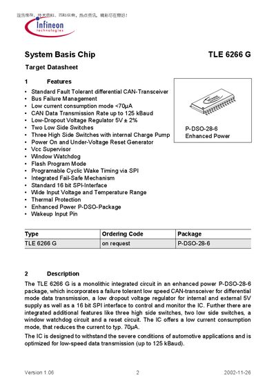
The TLE 6266 G is a monolithic System Basis Chip designed for automotive applications. It integrates a fault‑tolerant low‑speed CAN‑transceiver, a low‑dropout 5 V regulator, three high‑side switches, two low‑side switches, a window watchdog, and a 16‑bit SPI interface for control and monitoring.
The device offers four operation modes—normal, receive‑only, Vbat stand‑by and cyclic wake—selected via SPI bits. Detailed pin definitions, functional block diagrams and circuit descriptions are provided to aid designers in implementing the chip in safety‑critical systems.
| CAN data transmission rate | 125 kBaud |
|---|---|
| Low‑current consumption mode | 70 µA (typ.) |
| Low‑dropout voltage regulator | 5 V ±2 % |
| Low side switches | 2 |
| High side switches | 3 with internal charge pump |
| Window watchdog | Enabled |
| Fail‑safe mechanism | Integrated |
| Input voltage and temperature range | Wide |
The chip supports a CAN data rate of up to 125 kBaud.
It contains three high side switches with an internal charge pump.
Typical current consumption in the low‑current mode is about 70 µA.