
Key facts
- Brand
- Analog Devices
- Model
- AD9949
- Industry
- Industrial
- Documents
- 2
- Languages
- EN
- Last added
- 2012-05-09
Start here
Analog Devices AD9949 Datasheet
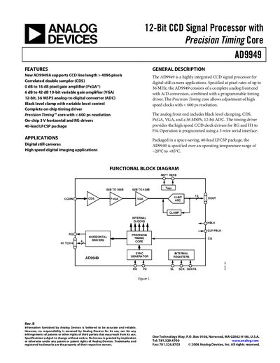
The AD9949 is a highly integrated 12‑bit CCD signal processor designed for digital still‑camera and high‑speed imaging applications. It combines a complete analog front‑end—including black‑level clamp, correlated‑double sampler, pixel‑gain (PxGA) and variable‑gain (VGA) amplifiers—with a 36 MS/s, 12‑bit ADC and on‑chip timing driver for CCD horizontal and reset‑gate clocks. Operation is controlled via a 3‑wire serial interface and the device is packaged in a 40‑lead LFCSP.
The part operates from –20 °C to +85 °C, with analog and digital supply voltages ranging from 2.7 V to 3.6 V. Key performance figures include a maximum clock rate of 36 MHz, 0 dB‑18 dB pixel‑gain range, 6 dB‑42 dB VGA range, 12‑bit resolution, DNL of –1.0 LSB to +1.0 LSB, and a typical power dissipation of 320 mW at 36 MHz.
Analog Devices AD9949 specifications
| Operating Temperature Range | -20 °C to +85 °C |
|---|---|
| Maximum Clock Rate | 36 MHz |
| Analog Supply Voltage (AVDD/TCVDD) | 2.7 V – 3.6 V (typical 3.0 V) |
| ADC Resolution | 12 bits |
| Pixel‑Gain Amplifier Range | 0 dB to 18 dB |
| Variable‑Gain Amplifier Range | 6 dB to 42 dB |
Source: Analog Devices AD9949 Datasheet
All Analog Devices AD9949 documents by type
Ratings, dimensions and ordering codes, for selection and design work.
Questions answered in these manuals
What is the maximum power dissipation at 36 MHz?
The device dissipates up to 320 mW at 36 MHz with HVDD = RGVDD = 3 V and 100 pF loading.
What is the recommended supply voltage for the analog front end?
The analog supplies (AVDD and TCVDD) should be between 2.7 V and 3.6 V, typically 3.0 V.
What is the operating temperature range of the AD9949?
The device operates from –20 °C to +85 °C.
What is the maximum clock rate supported by the AD9949?
The AD9949 can run at a maximum clock rate of 36 MHz.