
Key facts
- Brand
- Analog Devices
- Model
- AD5542A
- Category
- Other Electronics
- Documents
- 2
- Languages
- ZH · EN
- Last added
- 2026-10-01
Start here
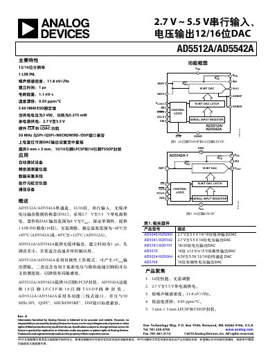
Analog Devices AD5512A/AD5542A DAC Datasheet
The AD5512A/AD5542A family provides single‑channel, 12‑ or 16‑bit resolution DACs with a wide supply range of 2.7 V to 5.5 V and unbuffered voltage output. They feature low noise (11.8 nV/√Hz), low temperature drift (0.05 ppm/°C) and a fast 1 µs settling time, making them suitable for high‑speed open‑loop control and precision instrumentation.
Typical applications include automatic test equipment, precision source‑measure instruments, data‑acquisition systems, medical and aerospace instrumentation, and communication equipment. The devices are offered in 10‑pin LFCSP, 16‑pin LFCSP and 16‑pin TSSOP packages and support SPI, QSPI, Microwire and DSP interfaces up to 50 MHz. This manual is written in Chinese.
Analog Devices AD5542A specifications
| Resolution | 12‑bit / 16‑bit |
|---|---|
| Power consumption (3 V supply) | 0.375 mW |
| Noise spectral density | 11.8 nV/√Hz |
| Temperature drift | 0.05 ppm/°C |
All Analog Devices AD5542A documents by type
Ratings, dimensions and ordering codes, for selection and design work.
Questions answered in these manuals
What is the DAC output voltage range?
The output can swing from 0 V up to the reference voltage (VREF).
What supply voltage does the AD5512A/AD5542A require?
Both devices operate from a single 2.7 V to 5.5 V supply.
How fast does the DAC settle to within ½ LSB?
The settling time is specified as 1 µs to reach ½ LSB of full scale.