
The AD9949 is a highly integrated CCD signal processor for digital still camera applications. Specified at pixel rates of up to 36 MHz, the AD9949 consists of a complete analog front end with A/D conversion, combined with a programmable timing driver. The AD9949 also features a Precision Timing™ core and other characteristics, making it suitable for digital cameras and high-speed digital imaging applications.
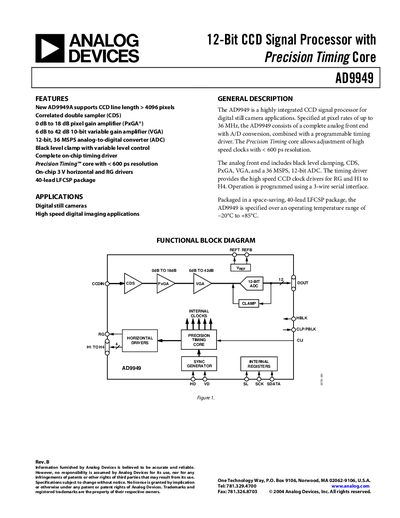
The AD9949 is a highly integrated 12‑bit CCD signal processor designed for digital still‑camera and high‑speed imaging applications. It combines a complete analog front‑end—including black‑level clamp, correlated‑double sampler, pixel‑gain (PxGA) and variable‑gain (VGA) amplifiers—with a 36 MS/s, 12‑bit ADC and on‑chip timing driver for CCD horizontal and reset‑gate clocks. Operation is controlled via a 3‑wire serial interface and the device is packaged in a 40‑lead LFCSP.
The part operates from –20 °C to +85 °C, with analog and digital supply voltages ranging from 2.7 V to 3.6 V. Key performance figures include a maximum clock rate of 36 MHz, 0 dB‑18 dB pixel‑gain range, 6 dB‑42 dB VGA range, 12‑bit resolution, DNL of –1.0 LSB to +1.0 LSB, and a typical power dissipation of 320 mW at 36 MHz.
| Operating Temperature Range | -20 °C to +85 °C |
|---|---|
| Maximum Clock Rate | 36 MHz |
| Analog Supply Voltage (AVDD/TCVDD) | 2.7 V – 3.6 V (typical 3.0 V) |
| ADC Resolution | 12 bits |
| Pixel‑Gain Amplifier Range | 0 dB to 18 dB |
| Variable‑Gain Amplifier Range | 6 dB to 42 dB |
The device dissipates up to 320 mW at 36 MHz with HVDD = RGVDD = 3 V and 100 pF loading.
The analog supplies (AVDD and TCVDD) should be between 2.7 V and 3.6 V, typically 3.0 V.
The serial interface supports a maximum SCK frequency of 10 MHz.
Pin 14 is the CCD Horizontal Clock 1 (H1) output.