
Key facts
- Brand
- Toshiba
- Model
- SSM3K09FU
- Industry
- Industrial
- Documents
- 2
- Languages
- EN
- Last added
- 2012-08-01
Start here
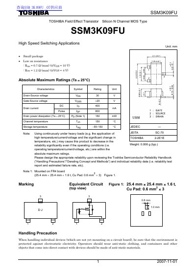
Toshiba SSM3K09FU Field Effect Transistor Datasheet
This document is a technical datasheet for the Toshiba SSM3K09FU, an N-channel silicon field effect transistor designed for high-speed switching applications. The device features a low on-resistance of 1.25Ω (typical) at Vgs = 4V and operates with a maximum drain-source voltage of 30V.
Read onlineToshiba SSM3K09FU specifications
| Drain-Source voltage (Vdss) | 30 V |
|---|---|
| Gate-Source voltage (Vgss) | +20 V |
| Drain current (Id) | 400 A |
| Pulse Drain current (Ipp) | 800 A |
| Drain power dissipation (Pd) | 150 mw |
| Channel temperature (Tch) | 150 °c |
| Gate threshold voltage (Vth) Min | 1.1 V |
| Drain-Source ON resistance (Rds(on)) Max @ 4V | 1.2 Ω |
| Drain-Source ON resistance (Rds(on)) Typ @ 3.3V | 1.0 Ω |
All Toshiba SSM3K09FU documents by type
Ratings, dimensions and ordering codes, for selection and design work.
Questions answered in these manuals
What is the maximum drain-source voltage?
The absolute maximum rating for the drain-source voltage is 30 V.
What is the typical on-resistance at 4V gate drive?
The typical on-resistance (Ron) is 1.25Ω when Vasg = 10 V, with a maximum of 1.2Ω at Vas = 4 V.
What is the maximum drain-source voltage?
The maximum drain-source voltage is 30 V.
From: TOSHIBA Field Effect Transistor Silicon N Channel MOS Type SSM3K09FU handbook
What is the maximum drain-source voltage rating?
The absolute maximum drain-source voltage rating is 30 V.
From: TOSHIBA Field Effect Transistor Silicon N Channel MOS Type SSM3K09FU handbook