
This document describes the features and characteristics of the SSM3K09FU field effect transistor from TOSHIBA. It is designed for high-speed switching applications and features a small package and low on-resistance.
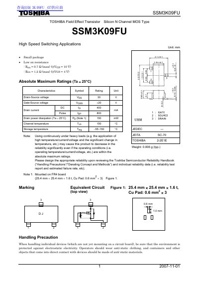
This document is a technical datasheet for the Toshiba SSM3K09FU, an N-channel silicon field effect transistor designed for high-speed switching applications. The device features a low on-resistance of 1.25Ω (typical) at Vgs = 4V and operates with a maximum drain-source voltage of 30V.
| Drain-Source voltage (Vdss) | 30 V |
|---|---|
| Gate-Source voltage (Vgss) | +20 V |
| Drain current (Id) | 400 A |
| Pulse Drain current (Ipp) | 800 A |
| Drain power dissipation (Pd) | 150 mw |
| Channel temperature (Tch) | 150 °c |
| Gate threshold voltage (Vth) Min | 1.1 V |
| Drain-Source ON resistance (Rds(on)) Max @ 4V | 1.2 Ω |
| Drain-Source ON resistance (Rds(on)) Typ @ 3.3V | 1.0 Ω |
The absolute maximum rating for the drain-source voltage is 30 V.
The typical on-resistance (Ron) is 1.25Ω when Vasg = 10 V, with a maximum of 1.2Ω at Vas = 4 V.
The device supports a pulse drain current of up to 800 A.