
Key facts
- Brand
- Maxim
- Model
- 105MSPS
- Industry
- Industrial
- Documents
- 2
- Languages
- EN
- Last added
- 2012-05-07
Start here
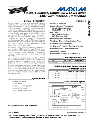
Maxim MAX1449 10-Bit 105Msps Single 3.3V Low-Power ADC with Internal Reference Datasheet
The MAX1449 is a 10‑bit analog‑to‑digital converter optimized for low‑power, high‑dynamic‑performance applications such as ultrasound imaging, CCD imaging, and digital set‑top boxes. It uses a pipelined 10‑stage architecture with a fully differential input stage, a wide‑band track‑and‑hold, and digital error correction. The device operates from a single 2.7 V to 3.6 V supply and includes a 2.048 V precision bandgap reference.
Typical specifications include a 105 Msps sampling rate, 58.5 dB SNR at 20 MHz, 72 dB SFDR at 20 MHz, and a -3 dB input bandwidth of 400 MHz. The MAX1449 is offered in a 32‑pin TQFP package (5 mm × 5 mm) and is rated for an industrial temperature range of –40 °C to +85 °C. Power consumption is 62 mA in normal operation and 5 µA in shutdown mode.
Maxim 105MSPS specifications
| Resolution | 10 Bits |
|---|---|
| Maximum Sampling Rate | 105 Msps |
| Supply Voltage | 3.3 V (typ) to 3.6 V |
| Power Consumption (Normal) | 62 mA |
| Power Consumption (Shutdown) | 5 µA |
| Input Bandwidth (-3 dB) | 400 MHz |
| Signal‑to‑Noise Ratio | 58.5 dB at 20 MHz |
| Spurious‑Free Dynamic Range | 72 dB at 20 MHz |
| Package | 32‑Pin TQFP, 5 mm × 5 mm |
| Operating Temperature Range | -40 °C to +85 °C |
| Internal Reference Voltage | 2.048 V |
| Output Type | CMOS‑compatible three‑state |
Source: Maxim MAX1449 10-Bit 105Msps Single 3.3V Low-Power ADC with Internal Reference Datasheet
All Maxim 105MSPS documents by type
Ratings, dimensions and ordering codes, for selection and design work.
Questions answered in these manuals
What is the maximum sampling rate of the MAX1449?
The MAX1449 can sample at up to 105 Msps (105 MHz).
From: Maxim MAX1449 10-Bit 105Msps Single 3.3V Low-Power ADC with Internal Reference Datasheet
What supply voltage does the MAX1449 require?
It operates from a single 2.7 V to 3.6 V supply, typically 3.3 V.
From: Maxim MAX1449 10-Bit 105Msps Single 3.3V Low-Power ADC with Internal Reference Datasheet
What is the maximum sampling rate of the MAX1180?
The MAX1180 can sample at up to 105 Msps.
From: Maxim MAX1180 Dual 10‑Bit 105Msps 3.3V Low‑Power ADC Data Sheet
What are the power consumption levels in normal, sleep, and shutdown modes?
Normal operation draws 125 mA, sleep mode 2.8 mA, and shutdown mode only 1 µA.
From: Maxim MAX1180 Dual 10‑Bit 105Msps 3.3V Low‑Power ADC Data Sheet