
Key facts
- Brand
- Maxim
- Model
- 170MSPS
- Industry
- Industrial
- Documents
- 2
- Languages
- EN
- Last added
- 2012-05-07
Start here
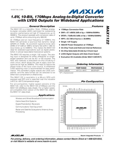
Maxim MAX1122 1.8V 10-Bit 170Msps Analog-to-Digital Converter with LVDS Outputs Datasheet
The MAX1122 is a monolithic 10‑bit, 170 Msps analog‑to‑digital converter optimized for high‑IF frequencies up to 500 MHz. It operates from a single 1.8 V supply, consumes about 460 mW at full speed, and provides LVDS‑compatible digital outputs selectable as two's complement or offset binary.
The device is offered in a 68‑pin QFN‑EP package, supports differential or single‑ended inputs, and includes on‑chip track‑and‑hold, an internal reference, and a selectable divide‑by‑2 clock circuit. It is specified for an industrial temperature range of –40 °C to +85 °C.
Maxim 170MSPS specifications
| Supply Voltage | 1.7 V – 1.9 V (AVcc/OVcc) |
|---|---|
| Resolution | 10 bits |
| Maximum Sampling Rate | 170 Msps |
| Power Dissipation | 460 mW at 170 Msps |
| Operating Temperature Range | -40 °C to +85 °C |
Source: Maxim MAX1122 1.8V 10-Bit 170Msps Analog-to-Digital Converter with LVDS Outputs Datasheet
All Maxim 170MSPS documents by type
Ratings, dimensions and ordering codes, for selection and design work.
Questions answered in these manuals
What is the maximum sampling rate of the MAX1122?
The MAX1122 can sample at up to 170 Msps.
From: Maxim MAX1122 1.8V 10-Bit 170Msps Analog-to-Digital Converter with LVDS Outputs Datasheet
What supply voltage range does the MAX1122 require?
Both the analog (AVcc) and digital (OVcc) supplies operate from 1.7 V to 1.9 V.
From: Maxim MAX1122 1.8V 10-Bit 170Msps Analog-to-Digital Converter with LVDS Outputs Datasheet
What is the maximum sampling rate of the MAX1213?
The MAX1213 can sample at up to 170 Msps.
From: Maxim MAX1213 1.8V 12‑Bit 170 Msps ADC for Broadband Applications Datasheet
What supply voltage does the MAX1213 require?
It operates from a single 1.8 V supply.
From: Maxim MAX1213 1.8V 12‑Bit 170 Msps ADC for Broadband Applications Datasheet