
Key facts
- Brand
- Texas Instruments
- Model
- CD74ACT10
- Category
- Other Electronics
- Documents
- 2
- Languages
- EN
- Last added
- 2012-07-02
Start here
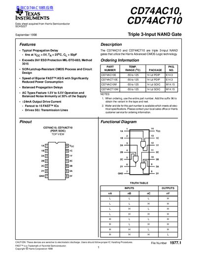
Texas Instruments CD74AC10/CD74ACT10 Triple 3-Input NAND Gate Datasheet
The document describes the CD74AC10 and CD74ACT10 devices as triple 3-input NAND gates utilizing Harris Advanced CMOS Logic technology. Key features include typical propagation delays of 6ns at 5V, SCR-latchup resistance, and operation ranges from 1.5V to 5.5V for AC types and 4.5V to 5.5V for ACT types.
Read onlineTexas Instruments CD74ACT10 specifications
| Typical Propagation Delay | 6ns at Voc = 5V, Ta = 25°C, CL = 50pF |
|---|---|
| Supply Voltage Range (ACT Types) | 4.5V to 5.5V |
| Operating Temperature Range | -55°C to 125°C |
| Output Drive Current | +24mA |
Source: Texas Instruments CD74AC10/CD74ACT10 Triple 3-Input NAND Gate Datasheet
All Texas Instruments CD74ACT10 documents by type
Ratings, dimensions and ordering codes, for selection and design work.
Questions answered in these manuals
What is the maximum propagation delay for the CD74AC10 at 5V?
The typical propagation delay is 12.2 ns when the supply voltage is 5V.
From: Texas Instruments CD74AC10/CD74ACT10 Triple 3-Input NAND Gate Datasheet
What is the maximum output drive current per pin?
The device provides a maximum output drive current of +24mA per output pin.
From: Texas Instruments CD74AC10/CD74ACT10 Triple 3-Input NAND Gate Datasheet
What is the supply voltage range for the CD54ACT109 and CD74ACT109?
The devices operate from –0.5 V up to 6 V.
What is the maximum clock frequency supported?
The maximum clock frequency is specified as 100‑114 MHz.