
CD54ACT109 and CD74ACT109 are dual J-K positive-edge-triggered flip-flops with clear and preset functions. They have TTL-voltage compatible inputs, balanced propagation delays, and reduced power consumption.
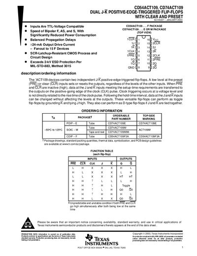
The CD54ACT109 and CD74ACT109 devices contain two independent J‑K positive‑edge‑triggered flip‑flops. A low level on the PRE or CLR inputs forces a set or reset, while normal operation transfers data on the rising clock edge when PRE and CLR are high. The devices can be used as toggle flip‑flops, D‑type flip‑flops, or standard J‑K flip‑flops.
The datasheet provides ordering information for PDIP, SOIC, and tube packages, electrical ratings such as supply voltage, output drive current, and thermal impedance, as well as timing parameters and switching characteristics. Packaging details, tape‑and‑reel dimensions, and TI’s important notice on product warranties and usage restrictions are also included.
| Supply voltage range | –0.5 V to 6 V |
|---|---|
| Output drive current | ±24 mA (fanout to 15 F devices) |
| Storage temperature range | –65 °C to 150 °C |
| Maximum clock frequency (fmax) | 100‑114 MHz |
| Setup time (tsu) | 5.5 ns (typical) |
| Hold time (th) | 0 ns |
The devices operate from –0.5 V up to 6 V.
The maximum clock frequency is specified as 100‑114 MHz.
The parts can be stored between –65 °C and 150 °C.
They can source or sink up to ±24 mA, allowing fanout to 15 F devices.