
Key facts
- Brand
- Maxim
- Model
- 250MSPS
- Industry
- Industrial
- Documents
- 4
- Languages
- EN
- Last added
- 2012-05-07
Start here
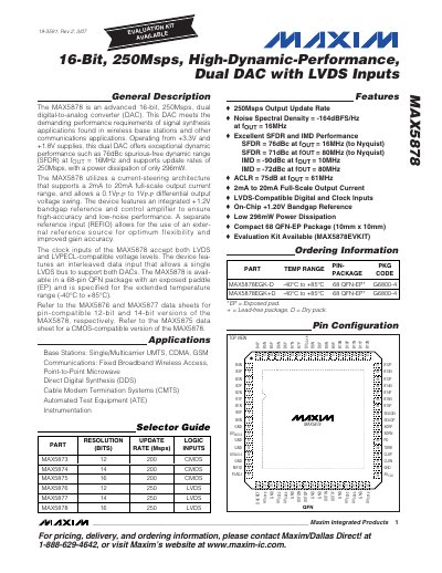
Maxim MAX5878 16‑Bit 250 Msps Dual DAC with LVDS Inputs Datasheet
The MAX5878 is an advanced 16‑bit, 250 Msps dual digital‑to‑analog converter designed for high‑dynamic‑performance signal synthesis in wireless base stations and other communications applications. It operates from +3.3 V and +1.8 V supplies and features a current‑steering architecture with a full‑scale output current range of 2 mA to 20 mA.
The device includes an integrated +1.2 V band‑gap reference, LVDS‑compatible clock and data inputs, and is offered in a 68‑pin QFN‑EP package rated for –40 °C to +85 °C. Detailed electrical characteristics, pin descriptions, and performance graphs are provided throughout the document.
Maxim 250MSPS specifications
| Resolution | 16 Bits |
|---|---|
| Output Update Rate | 250 Msps |
| Full‑Scale Output Current | 2 mA to 20 mA |
| Operating Temperature Range | -40 °C to +85 °C |
| Package | 68‑pin QFN‑EP |
| Noise Spectral Density | -164 dBFS/Hz at fOUT = 16 MHz |
| Spurious‑Free Dynamic Range (SFDR) | 76 dBc at fOUT = 16 MHz |
Source: Maxim MAX5878 16‑Bit 250 Msps Dual DAC with LVDS Inputs Datasheet
All Maxim 250MSPS documents by type
Ratings, dimensions and ordering codes, for selection and design work.
Questions answered in these manuals
What supply voltages does the MAX5878 require?
The device operates from +3.3 V analog and digital supplies and +1.8 V analog and digital supplies.
From: Maxim MAX5878 16‑Bit 250 Msps Dual DAC with LVDS Inputs Datasheet
What is the maximum output update rate of the MAX5878?
The DAC supports an output update rate of up to 250 Msps.
From: Maxim MAX5878 16‑Bit 250 Msps Dual DAC with LVDS Inputs Datasheet
What is the maximum output update rate of the MAX5876?
The MAX5876 supports an output update rate of 250 Msps.
From: Maxim MAX5876 12‑Bit 250Msps Dual DAC with LVDS Inputs Datasheet
How much power does the MAX5876 dissipate during normal operation?
Typical power dissipation is 287 mW.
From: Maxim MAX5876 12‑Bit 250Msps Dual DAC with LVDS Inputs Datasheet
What supply voltage does the MAX1121 require?
The MAX1121 operates from a single 1.8 V supply.
What is the maximum sampling rate of the MAX1121?
It can sample at up to 250 Msps.