
The MAX5878 is an advanced 16-bit, 250Msps, dual digital-to-analog converter (DAC) that meets the demanding performance requirements of signal synthesis applications found in wireless base stations and other communications applications. Operating from +3.3V and +1.8V supplies, this dual DAC offers exceptional dynamic performance such as 76dBc spurious-free dynamic range (SFDR) at fOUT = 16MHz and supports update rates of 250Msps, with a power dissipation of only 296mW. The MAX5878 utilizes a current-steering architecture that supports a 2mA to 20mA full-scale output current range, and allows a 0.1VP-P to 1VP-P differential output voltage swing. The device features an integrated +1.2V bandgap reference and control amplifier to ensure high-accuracy and low-noise performance. A separate reference input (REFIO) allows for the use of an exter- nal reference source for optimum flexibility and improved gain accuracy. The clock inputs of the MAX5878 accept both LVDS and LVPECL-compatible voltage levels. The device fea- tures an interleaved data input that allows a single LVDS bus to support both DACs. The MAX5878 is avail- able in a 68-pin QFN package with an exposed paddle (EP) and is specified for the extended temperature range (-40°C to +85°C). Refer to the MAX5876 and MAX5877 data sheets for pin-compatible 12-bit and 14-bit versions of the MAX5878, respectively. Refer to the MAX5875 data sheet for a CMOS-compatible version of the MAX5878.
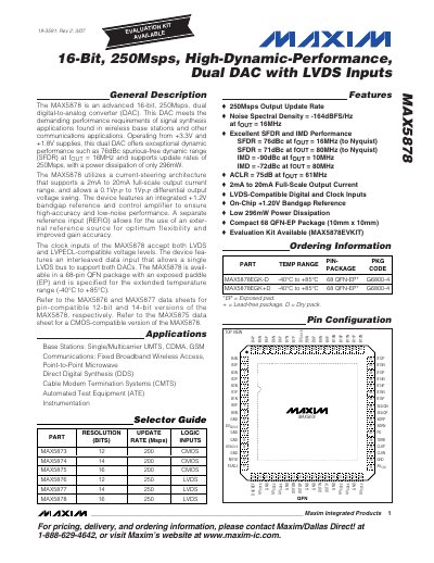
The MAX5878 is an advanced 16‑bit, 250 Msps dual digital‑to‑analog converter designed for high‑dynamic‑performance signal synthesis in wireless base stations and other communications applications. It operates from +3.3 V and +1.8 V supplies and features a current‑steering architecture with a full‑scale output current range of 2 mA to 20 mA.
The device includes an integrated +1.2 V band‑gap reference, LVDS‑compatible clock and data inputs, and is offered in a 68‑pin QFN‑EP package rated for –40 °C to +85 °C. Detailed electrical characteristics, pin descriptions, and performance graphs are provided throughout the document.
| Resolution | 16 Bits |
|---|---|
| Output Update Rate | 250 Msps |
| Full‑Scale Output Current | 2 mA to 20 mA |
| Operating Temperature Range | -40 °C to +85 °C |
| Package | 68‑pin QFN‑EP |
| Noise Spectral Density | -164 dBFS/Hz at fOUT = 16 MHz |
| Spurious‑Free Dynamic Range (SFDR) | 76 dBc at fOUT = 16 MHz |
The device operates from +3.3 V analog and digital supplies and +1.8 V analog and digital supplies.
The DAC supports an output update rate of up to 250 Msps.
It is available in a 68‑pin QFN‑EP package.