
The MAX1122 is a monolithic 10-bit, 170Msps analog-to-digital converter (ADC) optimized for outstanding dynamic performance at high IF frequencies up to 500MHz. The product operates with conversion rates of up to 170Msps while consuming only 460mW. At 170Msps and an input frequency of 100MHz, the MAX1122 achieves a spurious-free dynamic range (SFDR) of 72dBc. Its excellent signal-to-noise ratio (SNR) of 57.5dB at 10MHz remains flat (within 1dB) for input tones up to 500MHz. This makes the MAX1122 ideal for wideband applications such as digital predistortion in cellular base-station transceiver systems. The MAX1122 requires a single 1.8V supply. The analog input is designed for either differential or single-ended operation and can be AC- or DC-coupled. The ADC also features a selectable on-chip divide-by-2 clock circuit, which allows the user to apply clock frequencies as high as 340MHz. This helps to reduce the phase noise of the input clock source. A differential LVDS sampling clock is recommended for best performance. The converter’s digital outputs are LVDS compatible, and the data format can be selected to be either two’s complement or offset binary. The MAX1122 is available in a 68-pin QFN with exposed pad (EP) and is specified over the industrial (-40°C to +85°C) temperature range. For pin-compatible, higher speed versions of the MAX1122, refer to the MAX1123 (210Msps) and the MAX1124 (250Msps) data sheets.
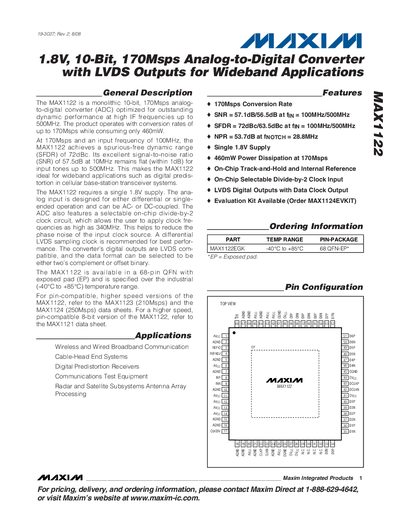
The MAX1122 is a monolithic 10‑bit, 170 Msps analog‑to‑digital converter optimized for high‑IF frequencies up to 500 MHz. It operates from a single 1.8 V supply, consumes about 460 mW at full speed, and provides LVDS‑compatible digital outputs selectable as two's complement or offset binary.
The device is offered in a 68‑pin QFN‑EP package, supports differential or single‑ended inputs, and includes on‑chip track‑and‑hold, an internal reference, and a selectable divide‑by‑2 clock circuit. It is specified for an industrial temperature range of –40 °C to +85 °C.
| Supply Voltage | 1.7 V – 1.9 V (AVcc/OVcc) |
|---|---|
| Resolution | 10 bits |
| Maximum Sampling Rate | 170 Msps |
| Power Dissipation | 460 mW at 170 Msps |
| Operating Temperature Range | -40 °C to +85 °C |
The MAX1122 can sample at up to 170 Msps.
Both the analog (AVcc) and digital (OVcc) supplies operate from 1.7 V to 1.9 V.
It is specified for an industrial temperature range of –40 °C to +85 °C.