
The MAX1213 is a monolithic, 12-bit, 170Msps analog-to-digital converter (ADC) optimized for outstanding dynamic performance at high-IF frequencies up to 300MHz. The product operates with conversion rates up to 170Msps while consuming only 788mW. At 170Msps and an input frequency up to 250MHz, the MAX1213 achieves a spurious-free dynamic range (SFDR) of 72.9dBc. Its excellent signal-to-noise ratio (SNR) of 66.2dB at 10MHz remains flat (within 2dB) for input tones up to 250MHz. This ADC yields an excellent low-noise floor of -68dBFS, which makes it ideal for wideband applications such as cable head-end receivers and power-amplifier predistortion in cellular base-station transceivers. The MAX1213 requires a single 1.8V supply. The analog input is designed for either differential or single-ended operation and can be AC- or DC-coupled. The ADC also features a selectable on-chip divide-by-2 clock circuit, which allows the user to apply clock frequencies as high as 340MHz. This helps to reduce the phase noise of the input clock source. A low-voltage differential signal (LVDS) sampling clock is recommended for best performance. The converter’s digital outputs are LVDS compatible and the data format can be selected to be either two’s complement or offset binary. The MAX1213 is available in a 68-pin QFN package with exposed paddle (EP) and is specified over the industrial (-40°C to +85°C) temperature range. See the Pin-Compatible Versions table for a complete list of part numbers.
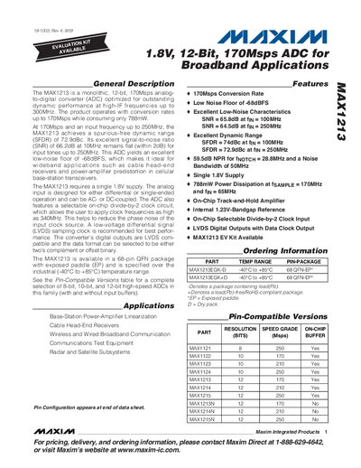
The MAX1213 is a monolithic 12‑bit ADC that operates from a single 1.8 V supply and delivers up to 170 Msps conversion rates. It offers low noise (‑68 dBFS), high dynamic range (SFDR up to 72.9 dBc) and supports both differential and single‑ended inputs, making it suitable for cable head‑end receivers, base‑station power‑amplifier linearization, and other wide‑band communication systems.
The device is offered in a 68‑pin QFN‑EP package, operates over an industrial temperature range (‑40 °C to +85 °C), and includes on‑chip features such as a selectable divide‑by‑2 clock, LVDS digital outputs, and an internal 1.23 V band‑gap reference. Ordering information, pin‑compatible family members, and detailed electrical characteristics are provided in the document.
| Conversion Rate | 170 Msps |
|---|---|
| Supply Voltage | 1.8 V (single supply) |
| Power Dissipation | 788 mW at 170 Msps |
| Input Frequency Range | up to 300 MHz |
| Package | 68‑pin QFN‑EP |
| Operating Temperature | -40 °C to +85 °C |
The MAX1213 can sample at up to 170 Msps.
It operates from a single 1.8 V supply.
At 170 Msps the device dissipates about 788 mW.