Maxim 65MSPS Manuals

We have 3 manuals for the Maxim 65MSPS: 2 Datasheets, 1 User Manual. Free to view online or download as PDF.

Maxim 65MSPS manuals

MAXIM MAX1211 65Msps 12-Bit IF Sampling ADC handbook

Datasheet

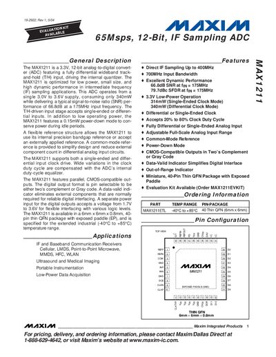
The MAX1211 is a 3.3V, 12-bit analog-to-digital converter (ADC) featuring a fully differential wideband track-and-hold (T/H) input, driving the internal quantizer. The MAX1211 is optimized for low power, small size, and high dynamic performance in intermediate frequency (IF) sampling applications. This ADC operates from a single 3.0V to 3.6V supply, consuming only 340mW while delivering a typical signal-to-noise ratio (SNR) performance of 66.8dB at a 175MHz input frequency. The T/H-driven input stage accepts single-ended or differential inputs. In addition to low operating power, the MAX1211 features a 0.15mW power-down mode to conserve power during idle periods. A flexible reference structure allows the MAX1211 to use its internal precision bandgap reference or accept an externally applied reference. A common-mode reference is provided to simplify design and reduce external component count in differential analog input circuits. The MAX1211 supports both a single-ended and differential input clock drive. Wide variations in the clock duty cycle are compensated with the ADC’s internal duty-cycle equalizer. The MAX1211 features parallel, CMOS-compatible outputs. The digital output format is pin selectable to be either two’s complement or Gray code. A data-valid indicator eliminates external components that are normally required for reliable digital interfacing. A separate power input for the digital outputs accepts a voltage from 1.7V to 3.6V.

MAXIM MAX1182 Dual 10-Bit 65Msps 3V Low-Power ADC with Internal Reference Parallel Outputs handbook

Datasheet

The MAX1182 is a 3V, dual 10-bit analog-to-digital con- verter (ADC) featuring fully-differential wideband track- and-hold (T/H) inputs, driving two pipelined, 9-stage ADCs. The MAX1182 is optimized for low-power, high- dynamic performance applications in imaging, instru- mentation and digital communication applications. This ADC operates from a single 2.7V to 3.6V supply, con- suming only 195mW while delivering a typical signal-to- noise ratio (SNR) of 59dB at an input frequency of 20MHz and a sampling rate of 65Msps. The T/H driven input stages incorporate 400MHz (-3dB) input amplifiers. The converters may also be operated with single-ended inputs. In addition to low operating power, the MAX1182 features a 2.8mA sleep mode as well as a 1µA power- down mode to conserve power during idle periods. An internal 2.048V precision bandgap reference sets the full-scale range of the ADC. A flexible reference structure allows the use of the internal or an externally derived reference, if desired for applications requiring increased accuracy or a different input voltage range. The MAX1182 features parallel, CMOS-compatible three-state outputs. The digital output format is set to two’s complement or straight offset binary through a single control pin. The device provides for a separate output power supply of 1.7V to 3.6V for flexible interfac- ing. The MAX1182 is available in a 7mm x 7mm, 48-pin TQFP package, and is specified for the extended industrial (-40°C to +85°C) temperature range.

MAXIM 14-Bit 65Msps 3.3V ADC MAX12553 Manual

User Manual

The MAX12553 is a 3.3V, 14-bit, 65Msps analog-to-digital converter (ADC) featuring a fully differential wideband track-and-hold (T/H) input amplifier, driving a low-noise internal quantizer. The analog input stage accepts single- ended or differential signals. The MAX12553 is optimized for low-power, small size, and high dynamic performance. Excellent dynamic performance is maintained from baseband to input frequencies of 175MHz and beyond, making the MAX12553 ideal for intermediate- frequency (IF) sampling applications. Powered from a single 3.15V to 3.60V supply, the MAX12553 consumes only 363mW while delivering a typical signal-to-noise (SNR) performance of 71dB at an input frequency of 175MHz. In addition to low oper- ating power, the MAX12553 features a 150µW power- down mode to conserve power during idle periods. A flexible reference structure allows the MAX12553 to use the internal 2.048V bandgap reference or accept an externally applied reference. The reference structure allows the full-scale analog input range to be adjusted from ±0.35V to ±1.10V. The MAX12553 provides a com- mon-mode reference to simplify design and reduce exter- nal component count in differential analog input circuits. The MAX12553 supports both a single-ended and dif- ferential input clock drive. Wide variations in the clock duty cycle are compensated with the ADC’s internal duty-cycle equalizer (DCE). ADC conversion results are available through a 14-bit, parallel, CMOS-com- patible, low-power, high-speed, low-noise output data bus.