
The MAX1182 is a 3V, dual 10-bit analog-to-digital con- verter (ADC) featuring fully-differential wideband track- and-hold (T/H) inputs, driving two pipelined, 9-stage ADCs. The MAX1182 is optimized for low-power, high- dynamic performance applications in imaging, instru- mentation and digital communication applications. This ADC operates from a single 2.7V to 3.6V supply, con- suming only 195mW while delivering a typical signal-to- noise ratio (SNR) of 59dB at an input frequency of 20MHz and a sampling rate of 65Msps. The T/H driven input stages incorporate 400MHz (-3dB) input amplifiers. The converters may also be operated with single-ended inputs. In addition to low operating power, the MAX1182 features a 2.8mA sleep mode as well as a 1µA power- down mode to conserve power during idle periods. An internal 2.048V precision bandgap reference sets the full-scale range of the ADC. A flexible reference structure allows the use of the internal or an externally derived reference, if desired for applications requiring increased accuracy or a different input voltage range. The MAX1182 features parallel, CMOS-compatible three-state outputs. The digital output format is set to two’s complement or straight offset binary through a single control pin. The device provides for a separate output power supply of 1.7V to 3.6V for flexible interfac- ing. The MAX1182 is available in a 7mm x 7mm, 48-pin TQFP package, and is specified for the extended industrial (-40°C to +85°C) temperature range.
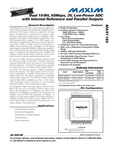
The MAX1182 is a dual‑channel 10‑bit analog‑to‑digital converter that operates from a single 2.7 V to 3.6 V supply. It provides fully‑differential wideband track‑and‑hold inputs, parallel CMOS‑compatible three‑state outputs, and an internal 2.048 V bandgap reference. The device is optimized for low‑power, high‑dynamic‑performance applications such as imaging, instrumentation and digital communications.
The ADC is offered in a 48‑pin TQFP‑EP package (7 mm × 7 mm) and is specified for an extended industrial temperature range (‑40 °C to +85 °C). It features selectable output format (two’s complement or offset binary), separate output supply (1.7 V‑3.6 V), and multiple power‑saving modes (sleep and shutdown).
| Supply Voltage Range (VDD) | 2.7 V – 3.6 V |
|---|---|
| Output Supply Voltage Range (OVDD) | 1.7 V – 3.6 V |
| Resolution | 10 bits |
| Maximum Sampling Rate | 65 Msps |
| Typical SNR (20 MHz input) | 59 dB |
| Normal‑Operation Power Consumption | 195 mW |
| Sleep‑Mode Current | 2.8 mA |
| Shutdown‑Mode Current | 1 µA |
| Internal Reference Voltage | 2.048 V |
| Package | 48‑pin TQFP‑EP, 7 mm × 7 mm |
The maximum clock frequency is 65 MHz.
In sleep mode the ADC draws 2.8 mA, and in shutdown mode it draws 1 µA.
The MAX1182 is supplied in a 48‑pin TQFP‑EP package measuring 7 mm × 7 mm.