
The MAX12553 is a 3.3V, 14-bit, 65Msps analog-to-digital converter (ADC) featuring a fully differential wideband track-and-hold (T/H) input amplifier, driving a low-noise internal quantizer. The analog input stage accepts single- ended or differential signals. The MAX12553 is optimized for low-power, small size, and high dynamic performance. Excellent dynamic performance is maintained from baseband to input frequencies of 175MHz and beyond, making the MAX12553 ideal for intermediate- frequency (IF) sampling applications. Powered from a single 3.15V to 3.60V supply, the MAX12553 consumes only 363mW while delivering a typical signal-to-noise (SNR) performance of 71dB at an input frequency of 175MHz. In addition to low oper- ating power, the MAX12553 features a 150µW power- down mode to conserve power during idle periods. A flexible reference structure allows the MAX12553 to use the internal 2.048V bandgap reference or accept an externally applied reference. The reference structure allows the full-scale analog input range to be adjusted from ±0.35V to ±1.10V. The MAX12553 provides a com- mon-mode reference to simplify design and reduce exter- nal component count in differential analog input circuits. The MAX12553 supports both a single-ended and dif- ferential input clock drive. Wide variations in the clock duty cycle are compensated with the ADC’s internal duty-cycle equalizer (DCE). ADC conversion results are available through a 14-bit, parallel, CMOS-com- patible, low-power, high-speed, low-noise output data bus.
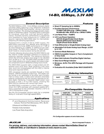
The MAX12553 is a 14‑bit, 65 Msps analog‑to‑digital converter optimized for low‑power, small‑size applications. It supports single‑ended or differential inputs, a flexible reference structure, and CMOS‑compatible parallel outputs selectable as two’s‑complement or Gray code.
The device is supplied from a single 3.15 V‑3.60 V rail, consumes 363 mW in differential‑clock mode, and offers a 150 µW power‑down mode. It is available in a 40‑pin thin QFN (6 mm × 6 mm × 0.8 mm) and operates over an extended industrial temperature range (‑40 °C to +85 °C).
| Resolution | 14 bits |
|---|---|
| Maximum Sampling Rate | 65 Msps |
| Supply Voltage | 3.15 V – 3.60 V |
| Power Consumption (Differential Clock) | 363 mW |
| Input Voltage Range | +0.35 V to +1.10 V |
| Signal‑to‑Noise Ratio (175 MHz) | 71 dB |
The MAX12553 can sample at up to 65 Msps.
In differential‑clock mode the device consumes 363 mW.
The full‑scale analog input can be adjusted from +0.35 V to +1.10 V.