
Key facts
- Brand
- Maxim
- Model
- 40MSPS
- Industry
- Industrial
- Documents
- 4
- Languages
- EN
- Last added
- 2012-05-07
Start here
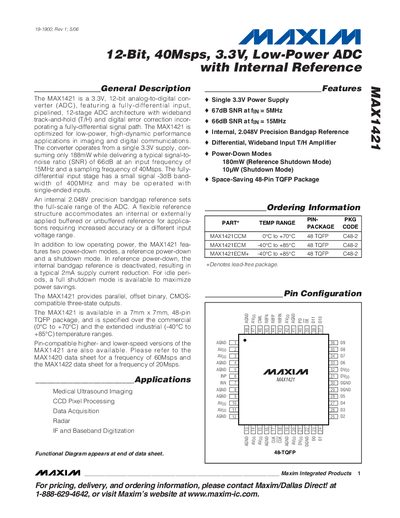
Maxim MAX1421 12‑Bit 40 Msps 3.3 V Low‑Power ADC with Internal Reference Datasheet
The MAX1421 is a 12‑bit, 40 Msps analog‑to‑digital converter optimized for low‑power, high‑dynamic‑range applications such as imaging and digital communications. It operates from a single 3.3 V supply, consumes only 188 mW, and provides a fully‑differential input path with a 400 MHz small‑signal bandwidth.
The datasheet lists electrical characteristics, absolute maximum ratings, timing parameters, and typical operating curves. It also includes ordering information, a 48‑pin TQFP package outline, pin configuration, and power‑down modes (reference shutdown and full shutdown).
Maxim 40MSPS specifications
| Resolution | 12 bits |
|---|---|
| Sampling Rate | 40 Msps |
| Supply Voltage | 3.3 V |
| Power Dissipation (typical) | 188 mW |
| Internal Reference | 2.048 V precision bandgap |
| SNR at 5 MHz | 67 dB |
| SNR at 15 MHz | 66 dB |
| Package | 48‑pin TQFP |
| Input Bandwidth | 400 MHz (-3 dB) |
| Power‑Down Modes | Reference shutdown 180 mW, full shutdown 10 pW |
Source: Maxim MAX1421 12‑Bit 40 Msps 3.3 V Low‑Power ADC with Internal Reference Datasheet
All Maxim 40MSPS documents by type
Ratings, dimensions and ordering codes, for selection and design work.
- Maxim MAX1421 12‑Bit 40 Msps 3.3 V Low‑Power ADC with Internal Reference Datasheet 17 p
- MAXIM MAX1183 Dual 10-Bit 40Msps 3V Low-Power ADC with Internal Reference Parallel Outputs handbook 18 p
- Maxim MAX1195 Dual 8‑Bit 40Msps 3V Low‑Power ADC Datasheet 22 p
- Maxim MAX1126 Quad 12‑Bit 40Msps ADC Datasheet 26 p
Questions answered in these manuals
What supply voltage does the MAX1421 require?
The MAX1421 operates from a single 3.3 V supply.
From: Maxim MAX1421 12‑Bit 40 Msps 3.3 V Low‑Power ADC with Internal Reference Datasheet
What power‑down modes are available for the MAX1421?
It offers a reference shutdown mode (180 mW) and a full shutdown mode (10 pW).
From: Maxim MAX1421 12‑Bit 40 Msps 3.3 V Low‑Power ADC with Internal Reference Datasheet
What is the operating supply voltage range for the MAX1183?
The device operates from 2.7 V to 3.6 V analog supply voltage.
From: MAXIM MAX1183 Dual 10-Bit 40Msps 3V Low-Power ADC with Internal Reference Parallel Outputs handbook
Can the output data format be changed?
Yes, the output format can be set to two’s complement or straight offset binary via a single control pin.
From: MAXIM MAX1183 Dual 10-Bit 40Msps 3V Low-Power ADC with Internal Reference Parallel Outputs handbook
What is the operating supply voltage range of the MAX1195?
The MAX1195 operates from a single supply of 2.7 V to 3.6 V.
From: Maxim MAX1195 Dual 8‑Bit 40Msps 3V Low‑Power ADC Datasheet
How much power does the MAX1195 consume in normal operation?
In normal operation the device consumes 87 mW.
From: Maxim MAX1195 Dual 8‑Bit 40Msps 3V Low‑Power ADC Datasheet