
Key facts
- Brand
- Analog Devices
- Model
- AD5301
- Industry
- Industrial
- Documents
- 2
- Languages
- EN
- Last added
- 2012-05-09
Start here
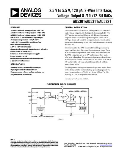
Analog Devices AD5301/AD5311/AD5321 DAC Datasheet
The AD5301/AD5311/AD5321 family provides single‑chip buffered voltage‑output DACs ranging from 8‑ to 12‑bit resolution. They operate from a 2.5 V to 5.5 V supply, consume only 120 µA at 3 V in normal mode, and feature a rail‑to‑rail output buffer with a 0.7 V/µs slew rate. Communication is via a 2‑wire I²C‑compatible serial interface that supports clock rates up to 400 kHz and allows multiple devices on the same bus.
The datasheet includes detailed specifications such as resolution, accuracy, power‑down modes, pin configurations, timing diagrams, and absolute maximum ratings. Typical applications include portable battery‑powered instruments, programmable voltage sources, and digital gain/offset adjustment circuits.
Analog Devices AD5301 specifications
| Supply Voltage Range | 2.5 V to 5.5 V |
|---|---|
| Resolution (bits) | 8‑10‑12 (AD5301/AD5311/AD5321) |
| Power‑down Current | 50 nA @ 3 V |
| Maximum I²C Clock Frequency | 400 kHz |
| Short‑Circuit Output Current | 50 mA (5 V) |
All Analog Devices AD5301 documents by type
Ratings, dimensions and ordering codes, for selection and design work.
Questions answered in these manuals
What supply voltage does the AD5301 family require?
The devices operate from a 2.5 V to 5.5 V supply.
How many bits of resolution does the AD5311 provide?
The AD5311 provides 10‑bit resolution.
What is the supply voltage range for the AD5301/AD5311/AD5321?
The devices operate from 2.5 V to 5.5 V.
How much current does the DAC draw in power‑down mode at 3 V?
Power‑down current is 50 nA at 3 V.